I’ve spent the last several weeks staring into my light table and generating board designs. Most of these designs are replicas of designs I have the real boards for. That is mostly for complete-ness and to have the designs in KiCAD for ease of diagnosing problems and seeing what net each trace belongs to. Some of those designs are for boards I only know of being in a literal museum and I don’t know how it’s wired or what it does. Through this exercise of generating schematics for all these boards I have come up with some interesting information for how they all work and I’m going to share that here across several entries.
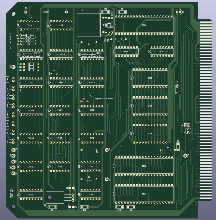
The first board I’m going to talk about is the CPU board for the Chuck-E-Cheese Cyberamic Control Computer. The first generation of this card was designed some time around 1979 according to the schematics and has some design choices that you might recognize. It is made up of a 6502 processor, two 6532 RIOT chips for the RAM, stack, timers, and some I/O, and three 2708 EPROM chips for storing the program. This board fits into a card cage, and only in one specific card slot. This backplane does not have a bunch of parallel wired slots like you might find in an s100 computer of the era, it has a couple large slots for the CPU, Transport, and Audio cards to be installed as well as a bunch of identical slots for character and lights cards to be installed depending on the show configuration.
The processor here has an interesting feature in that the address bus was not fully utilized. Lines A13-A15 were not connected anywhere limiting the memory space of the 6502 from 64K down to 8K. If I were designing a backplane I might try to find room for those three extra lines in case I wanted to expand it more later, but for some reason these designers thought that 8K of memory space was enough. The Interrupt line is wired out to the backplane, but on the backplane I have, it’s not connected to anything. Even if one of the other cards was also wired up, this feature couldn’t be used. Those features along with the use of RIOT chips for RAM have me thinking of one thing. This thing is an overgrown Atari 2600. It’s true, Chuck-E-Cheese’s Pizza Time Theater was created as a child friendly place to have Atari arcade games and the design of their in-house animatronics controller shows it.
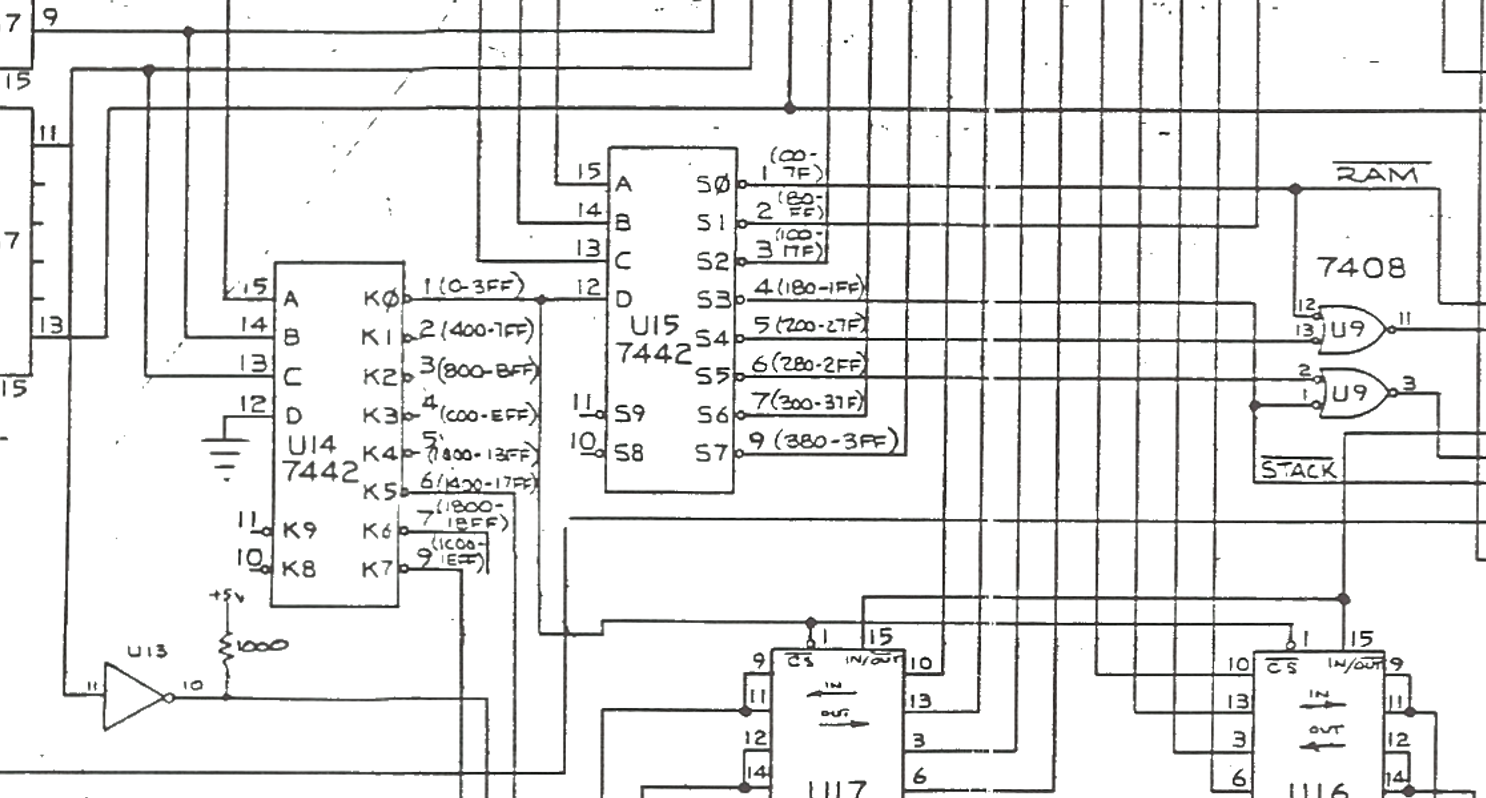
The inputs to this board include a microphone switch, a bunch of buttons that were mounted on the front of the machine (located in a regular 19″ rack), and a rotary switch to set the intensity of the ‘automatic gain control’ for the volume of the show. The outputs are the lights behind the buttons, some lights on the edge of the card that can be used to tell what state it is in, or diagnose problems, and of course driving all the rest of the cards in the system. The address decoding was done by some 7442 chips and each output card only got 8 addresses because they were selected with Address A2-A5. The other sections of memory dedicated to the transport card, the audio card, the I/O, etc.. got 128 addresses per (that’s how much RAM this thing had, but it also had that much stack in the other RIOT chip). The ROMs being 2708s had 1K per and were mapped in at $1400 to $1FFF. How does that work when the 6502 boots from $FFFC and $FFFD? well, not using those last three address lines means that the entire memory map is ‘mirrored’ so that you have multiple copies of the same information logically located all over the memory map. Reading from $FFFC gets the same data as from $1FFC, which is in ROM U20.
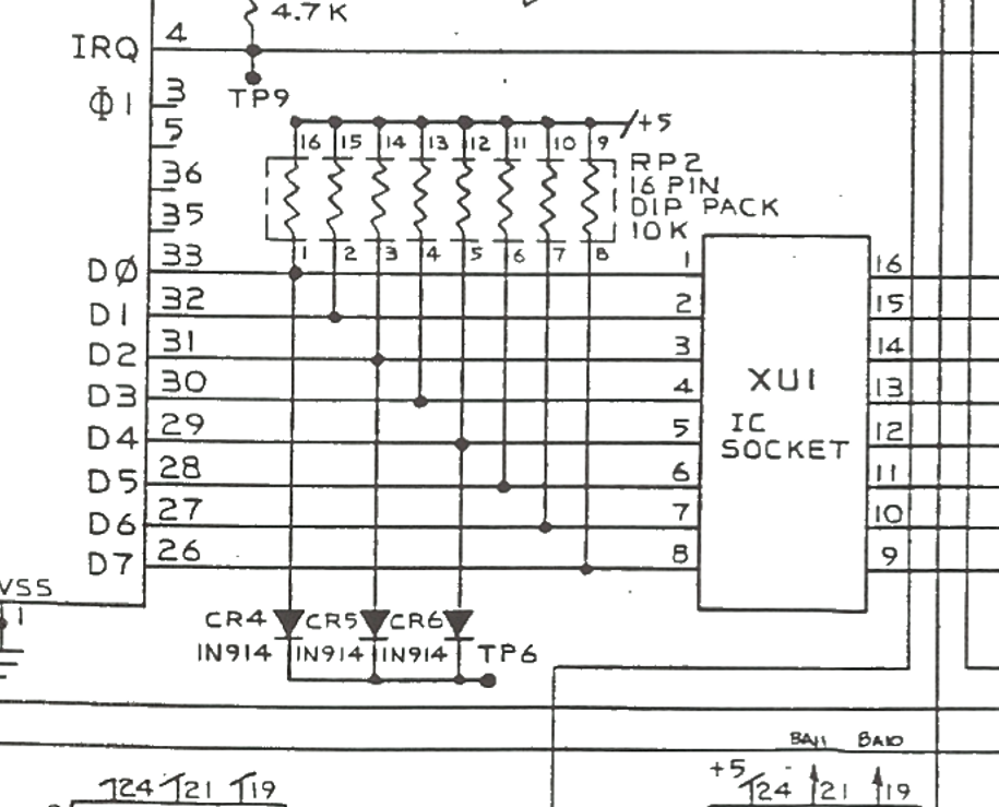
There’s also some other cool features of this board. If you want to test that the CPU is working you can remove the jumper at socket XU1 to disconnect the data bus from the CPU and then ground TP6. This makes the CPU execute a NOP instruction continuously thereby allowing you to see if it’s working (the address bus should be constantly counting up). There is a ‘hold’ input to this board allowing other cards in the backplane to effectively ‘pause’ the CPU execution.
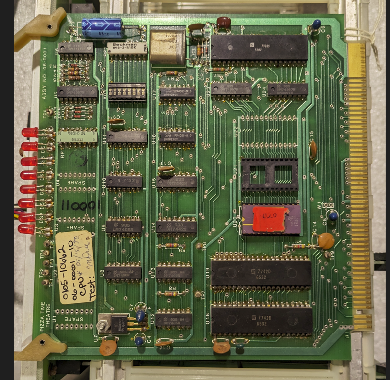
I didn’t have one of these boards to work with, but I had a lot of pictures from three in the San Jose History museum and a couple of schematics to look at. You might think that the schematics are the holy grail, but in the days before CAD, there are frequently mistakes. Heck, in the days of CAD there are still mistakes. Utilizing all three variations of the CPU card that I had pictures of and both sets of schematics I was able to recreate the CPU card 06-0001 revisions A-D.
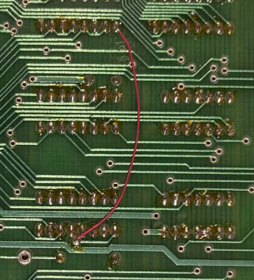
Revision A is the earliest and had several errors on the PCB. Two traces are missing and jumpered to make it work. One trace is made incorrectly and was cut and pulled up. The ground is not fully connected to itself (but since this goes in a backplane that connects it for us). Some pins the schematic claims are grounded are not, that has no effect on performance.
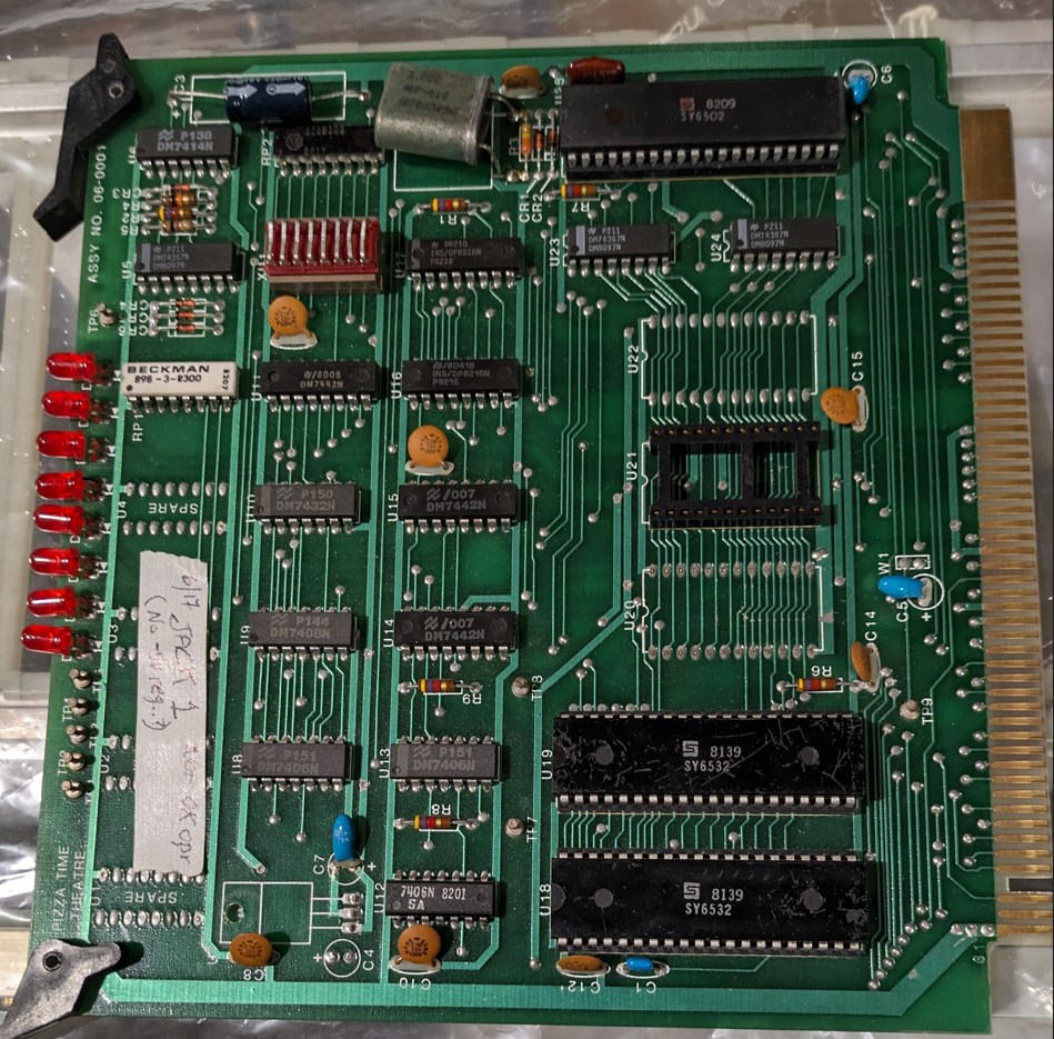
Revision B, according to the paper schematic changelog made one capacitor 16v instead of 10v. This is partially true, but they also fixed the cut and jumpered traces from revision A. They didn’t fix the grounding issues, possibly because they didn’t know about them, and overall this board design seems to be in a good state.
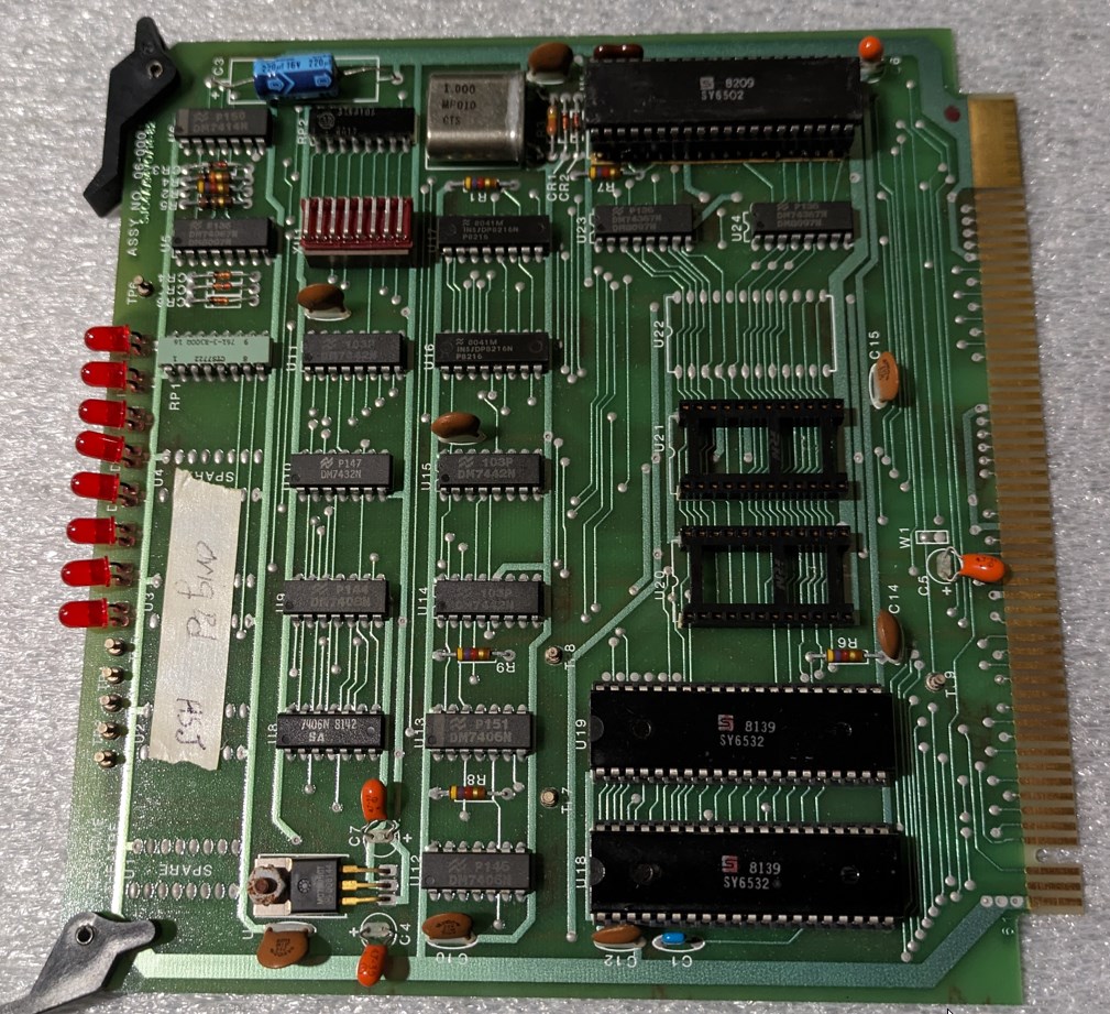
Revision C claims ‘added ref. callouts’ but I don’t know what this could mean as the later schematic has the same reference designators as the earliest one and the board silkscreen is unchanged. The version is incremented in the copper layer text though.
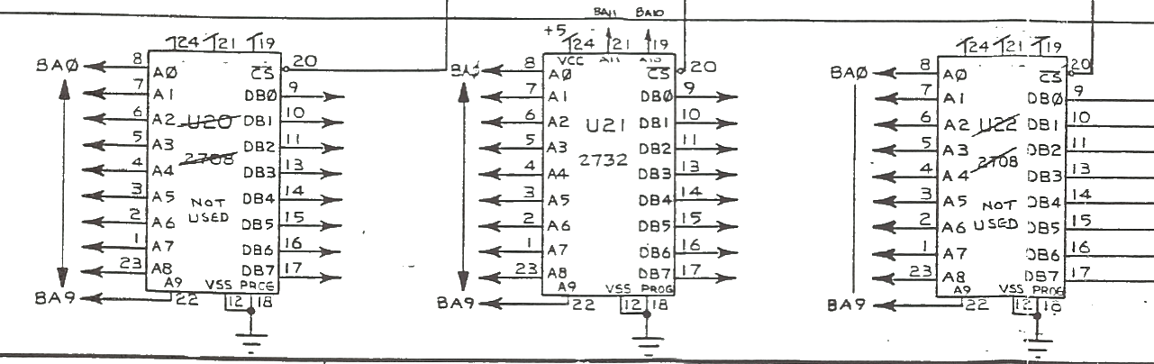
Revision D I have only seen in schematic form and in the way other older revision boards have been modified. This version removes the capability of using 2708 chips and instead substitutes a 2732 chip. The decoding logic is changed to just whenever A12 is high, the 2732 is selected, effectively replacing the 3 2708 chips’ location exactly and adding 1K more memory before each block. The rewiring makes two memory chip sockets useless and reuses the middle one for the 2732. I have seen this mod executed on the revision B board, but never a real one with the traces implemented. To design this one I took a best guess and I think it came out alright. If you’re going to have one of these boards manufactured and you don’t need to remain compatible with a 2708 ROM then I suggest the revision D. I also took the chance to correct the grounding issues because they bugged me (although the real one probably did not).
The 1993 redesign of this system say revision HA, which changed the whole board to use an HC11 processor and also modified the remainder of the data and audio subsystem so it remains compatible only with the old character and light driver cards. I haven’t remade this one because I’m not super interested in rebuilding that era of system, but it’s possible and I have the card to copy.
If you need one of these board I can make you one, or you can find the design up on github here. This goes along with the adapter I made to connect the buttons and lights to the backplane. I will have more details on how the other subsystems work and which versions are compatible with each other coming up. Feel free to ask me about any issues you may have with one of these setups. I may know something after digging so deep into all this.

April 3, 2024 at 1:48 am |
[…] third board I’m going to try to explain is the audio board. This one was harder to do than the […]
April 9, 2024 at 9:27 am |
[…] You can read all the details in the post here. […]