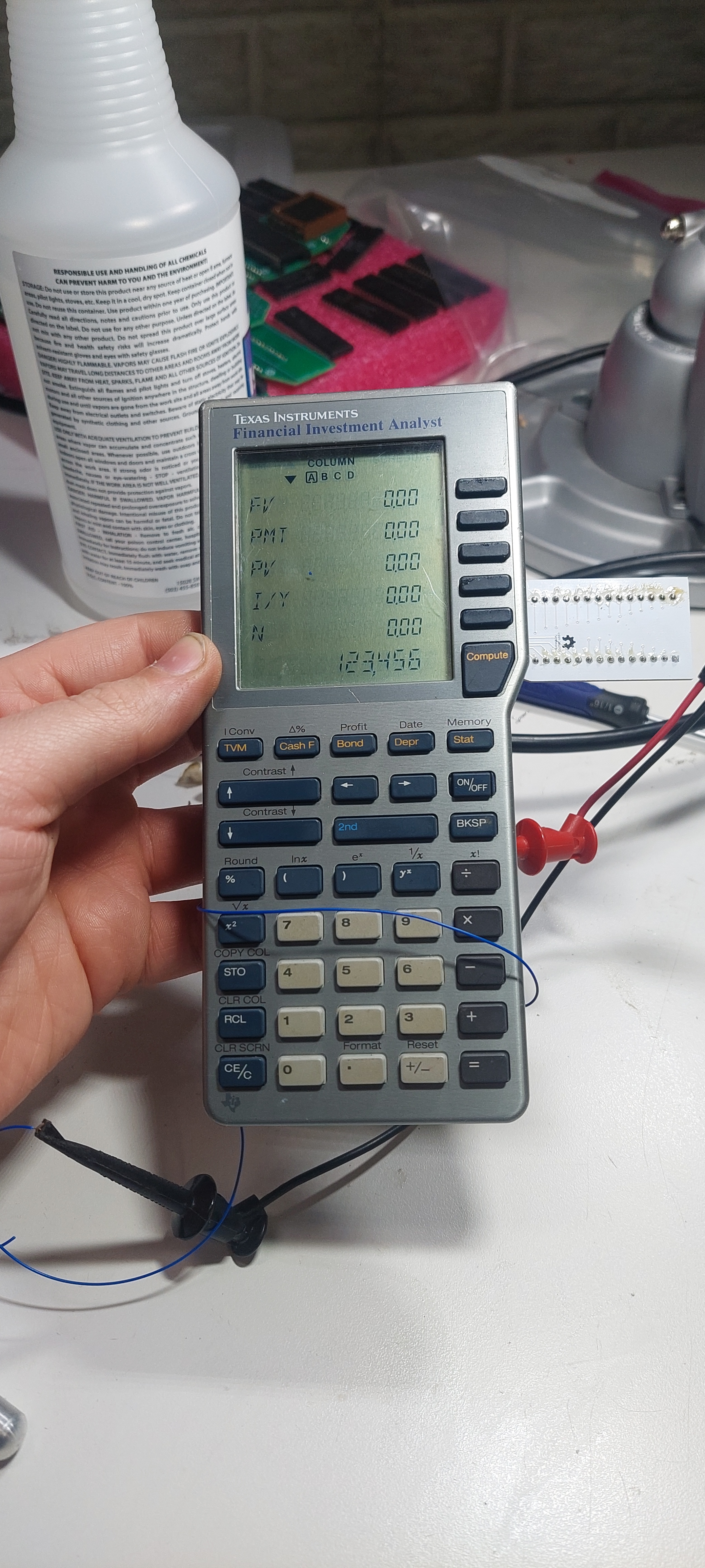
This is a somewhat generic idea, but I’ve implemented it for a specific purpose. In trying to be able to dump all the TMS7000 series processors’ internal mask rom I’ve come across some pretty unique ones. The latest ones are the TMS70C46 processors found in the TI-74 basicalc and the FIA-10 financial calculator. These calculators seem to contain internal mask rom, but they also have built in address decoding to select different memory chips for different regions of memory.
This makes it more difficult to capture any of the reads to external memory because now we need to know which region it’s trying to read. I attempted to diode-or these together and use the standard dumper we have been using, but that didn’t work and it’s hard to know why. I am fairly confident that for the FIA-10 I know where it either executes all of its code from, or where it gets at least some from: the external mask rom.
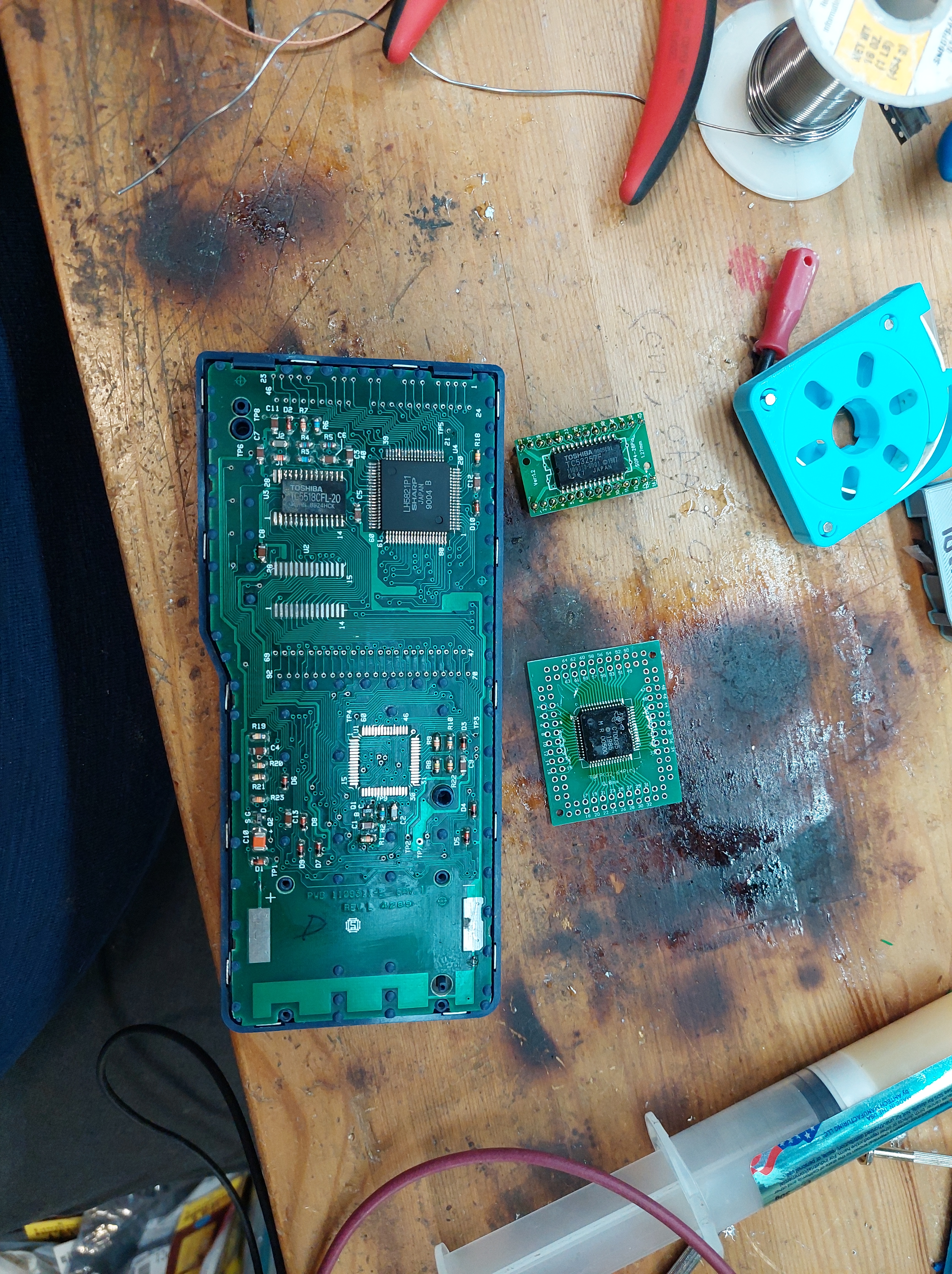
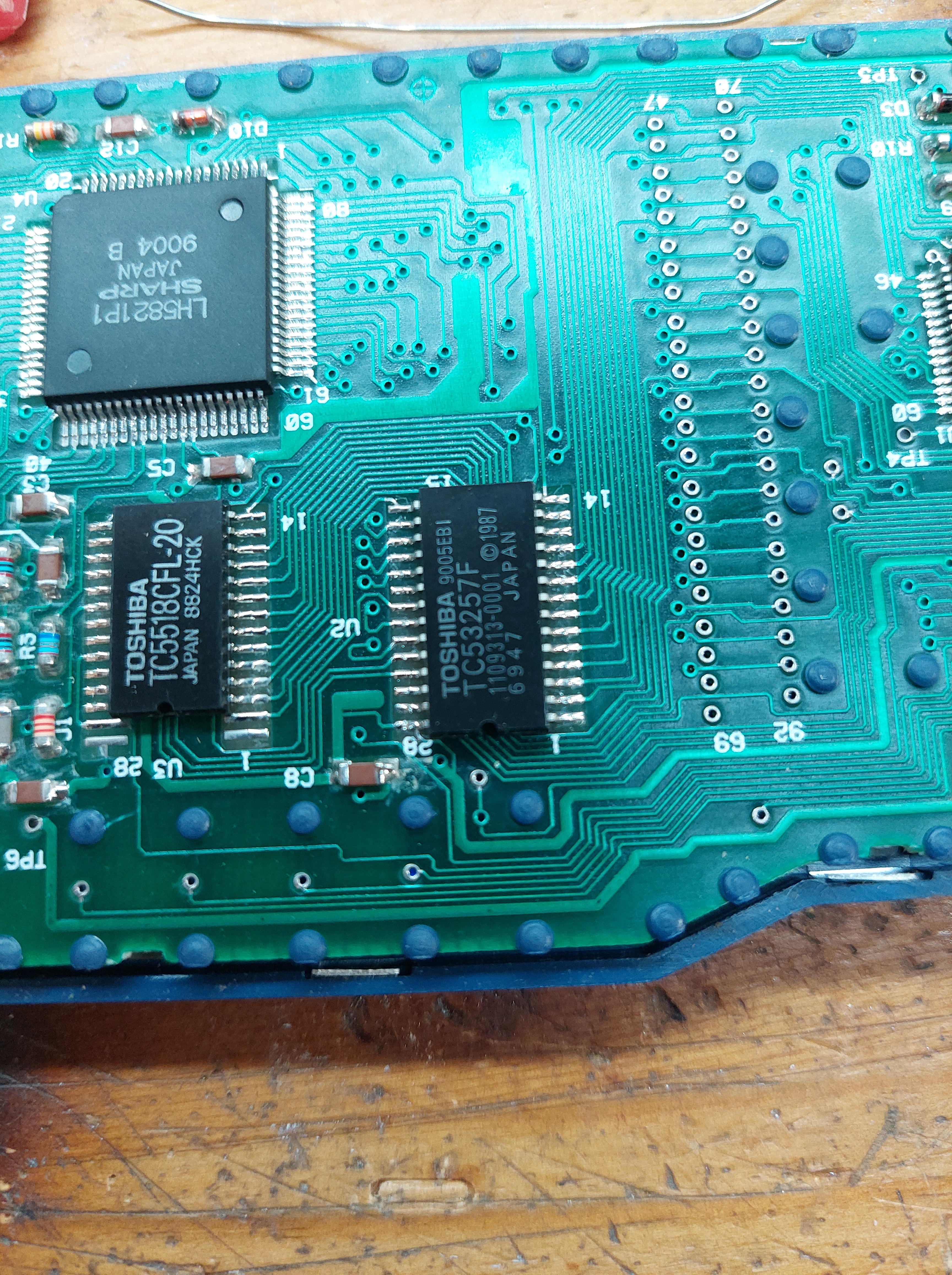
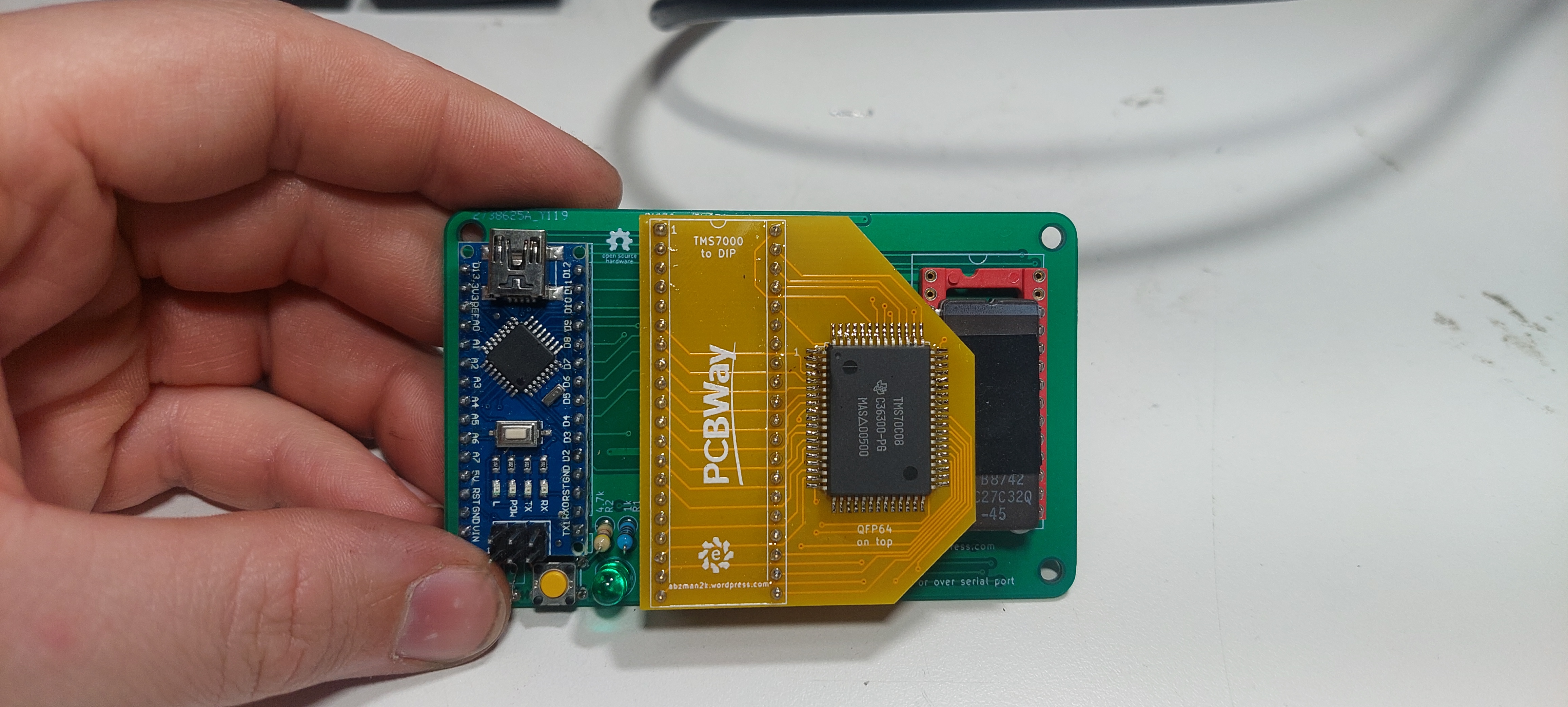
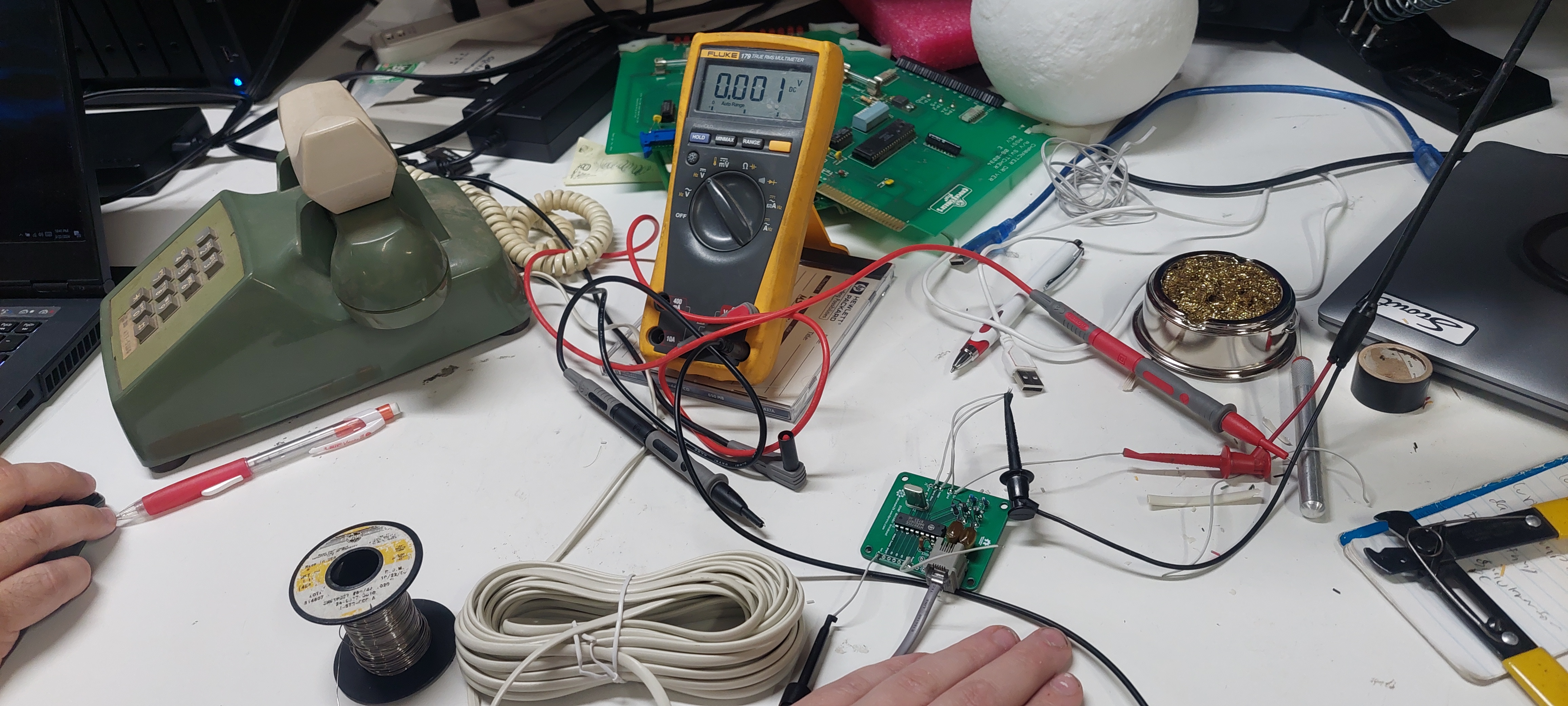
I have already desoldered this ROM to read the contents, but now I want to put my own code there. Not just code, it would be very convenient to actually talk to the processor and command reads and writes to different regions to see what happens. I have a way to do this, it’s called Demon Debugger. There isn’t a target for the tms7k yet, but that part shouldn’t be too hard. What I need now is a way to get our code into the processor. Our latest version of Demon Debugger fits where a standard 2716 would go and uses certain regions for input and output so we could just replace the external mask rom if we know what area it’s trying to read. But how do I cable that in to this SOIC chip?
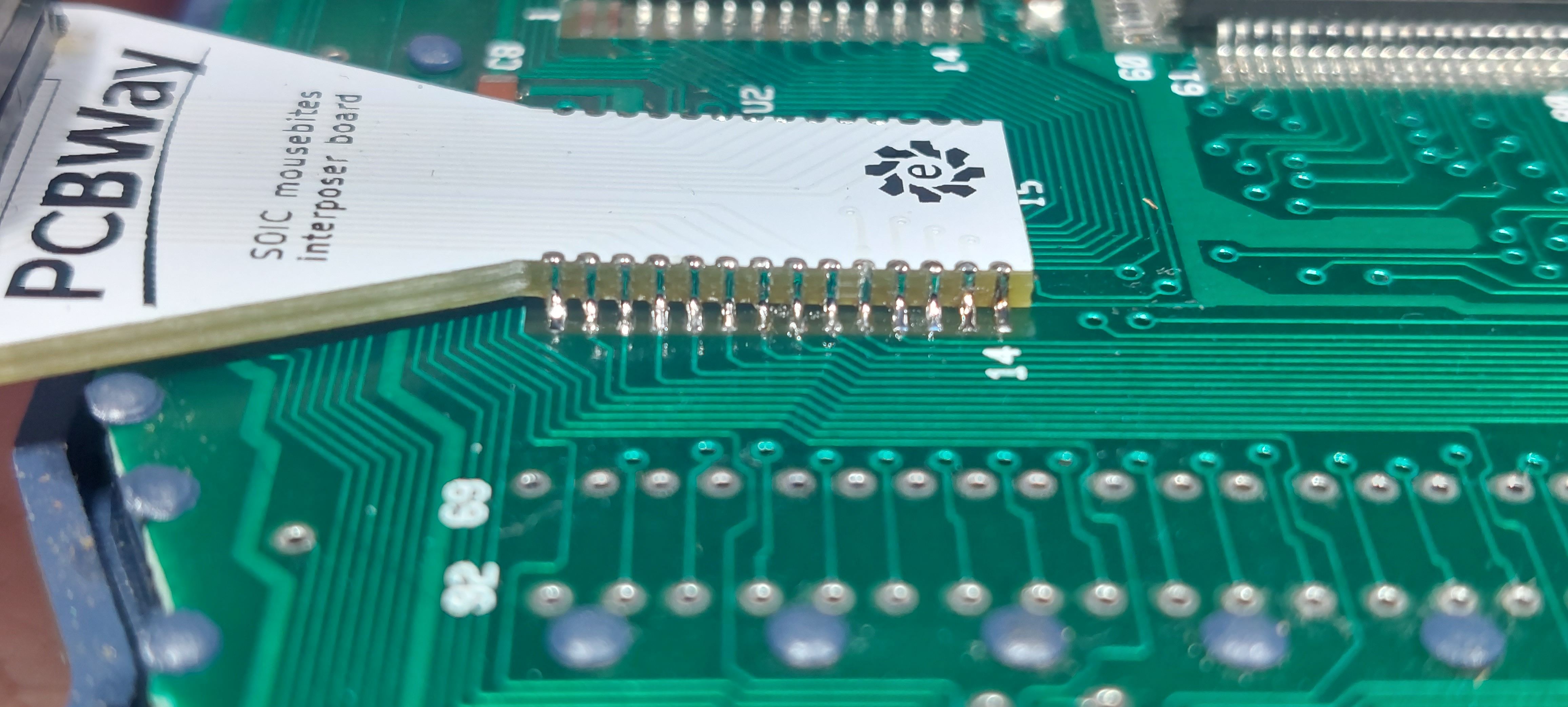
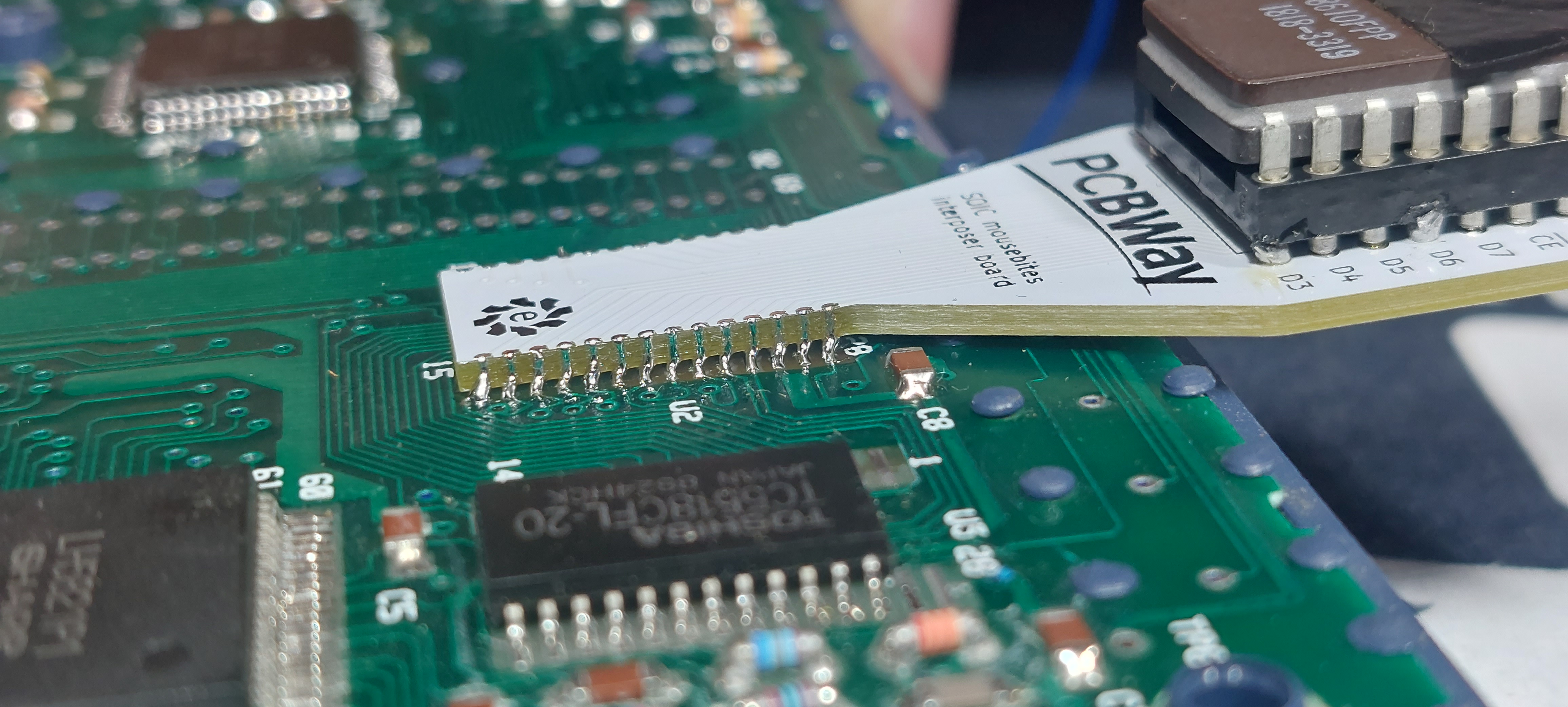
This is the latest board I got sponsored by PCBWay. This is what I’m calling the ‘mousebites’ adapter. That’s the term I’ve seen for castelated pins on the side of a board, and I think it’s cute. I used the datasheet for the exact mask rom that was installed there to get all the measurements needed to line up my board so it can be soldered where the rom chip used to be.
After installing this I realized it would be a perfect use case for a flexible PCB, but I didn’t notice the plastic bumps securing the board before I got this installed. That being said I got this one made in white with black silkscreen and that looks very sharp. I can tell why most boards tend to be green, because I can’t see the traces on the board as well with the white. The silkscreen on the soldermask though, that’s very distinct with this color combination. If you’re going to enter PCBWay’s 10th aniversary contest, this could be a good choice for your design. That is if you don’t want to venture into their full color printing.
This is what it looks like with a standard rom in the socket that I intend to use for demon debugger. It’s fairly rigid, but with all that leverage I’m afraid it’s going to rip traces right off the board. In order to prove it works as-is I put the same data from the mask rom on a standard 27256 to see if it’ll boot.
And it does! This sort of adapter has many uses, but unfortunately the orientation is pretty specific. I designed this one to stick out the edge of the calculator. If the orientation were flopped it would not work at all. If I made this as a flex pcb it would be more generic, but even then it’s not a sure thing. As it is this one works and I’ll be interested to see how It works with demon debugger.
Do not use git branches, this is a way to lose shit you’ve been working on. Do not use git stashes, this is a way to lose shit you’ve been working on *and it’s not backed up anywhere*. Git is just too complicated to use all of it and expect to not lose stuff. I’m trying to get back into this project after an entire year and figuring out where we left off and what was going wrong has been a whole ordeal.
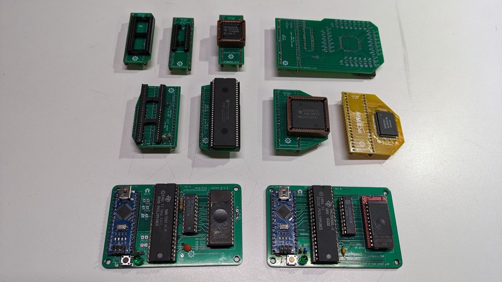
This is the resumption of a project on dumping the internal contents of the tms7000 processor. Over a year ago we had moved on from the hardware SPI implementation of the revision A to the parallel approach of revision B. I don’t recall why we moved to a parallel interface, but I think it had to do with one of the pincount reduced chips not being compatible with our original SPI method. I think the later bigger chips are also not compatible with SPI though, so I’ll update this when I find out. The board with no revision had no ability to detect CMOS/NMOS and had a different resistor value for the LED. Revision A added those, and revision B changed from SPI to parallel.
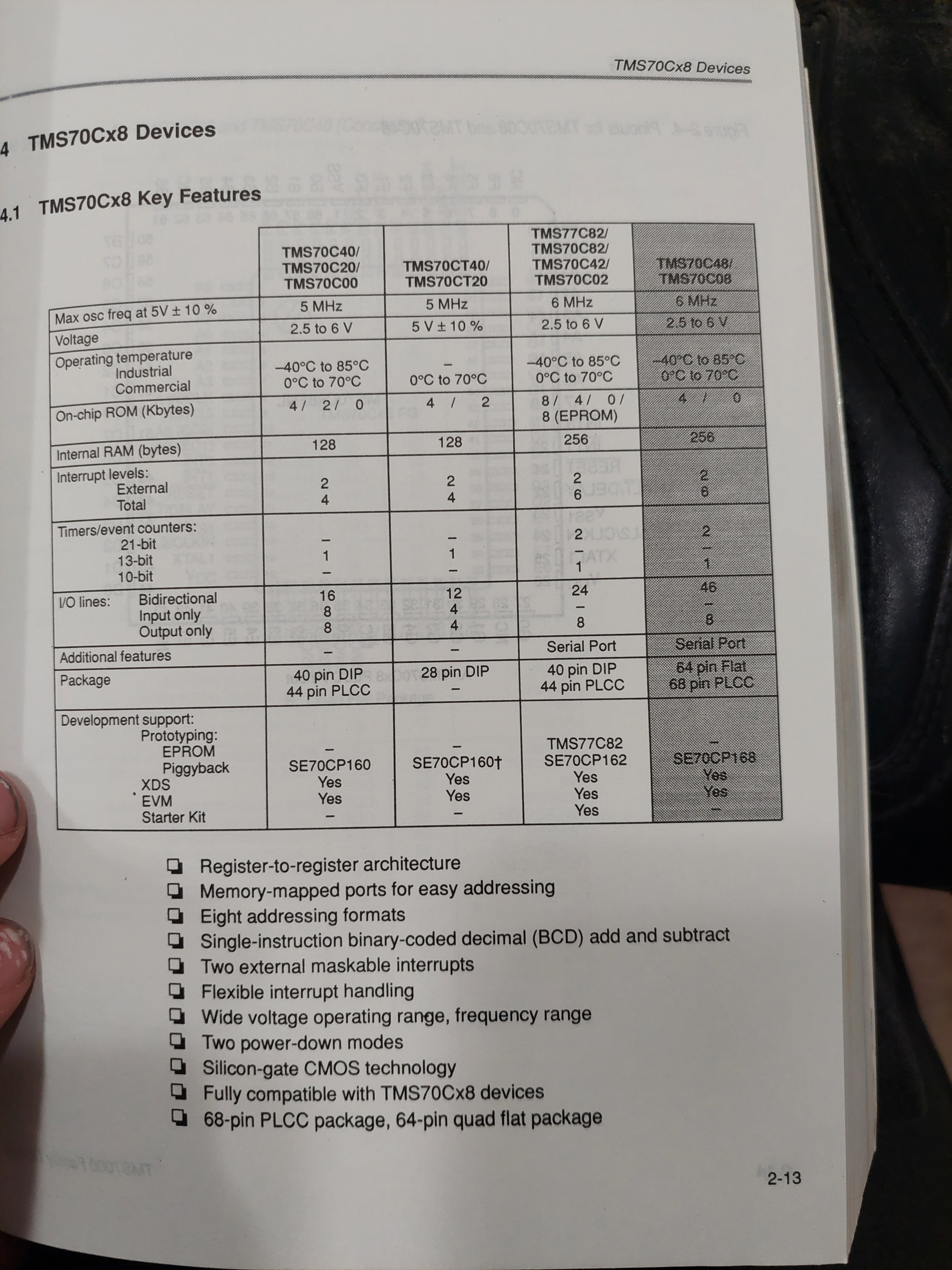
In the interim since the last update we have been designing adapters for a whole new series of chips. The 7xx8 chips. These are bigger pincount chips that seem to be one of the last sort of tms7000 around. They look like they were more popular in europe and that’s where we found this databook. This is a 1991 version of the tms7000 databook and it’s not scanned or on bitsavers yet. I’d like to do that at some point, but for now I took pictures of the most interesting sections and they are up on my github.
The board was designed specifically to work with the DIP40 variant of the tms7000 but we now have adapters to successfully dump the:
DIP 28 0.07″ pitch
DIP 40 0.07″ pitch
DIP 64 0.07″ pitch
DIP 64
PLCC 44
PLCC 68
QFP 64
Today’s PCBWay sponsored board is this nice QFP64 adapter. It worked first try because the chip inside is basically the same as everything else, I just used the new databook to connect the dots. I got this one in a stylish yellow. I think it looks just as good as yesterday’s red, but in an unexpected way. This is one that you might think at first glance is a flex PCB, but it’s not.
There is a problem with the tms7000 dumpers we have though. rev.A only works on the 40 pin, and 44 pin chips. rev.B theoretically works on all of them, but it has issues locking up on certain 40 pin chips though. We’re not 100% sure why, but it may have to do with the fact we’re clocking the chip and we don’t do it fast enough to keep the memory alive in certain ones. So we have this conundrum, all* chips can be dumped, but not with one universal dumper. This is a problem we’re actively working on and hope to get it solved soon. We have a lot of chips purchased from ebay and dumps of them all up on github so we can test until they all work. An interesting aspect about this project is they all have internal rom. Ignore the part number printed on the chip, they all have some sort of mask rom. We have even found some that we think are factory test roms and are loaded in multiple different package chips we got from different sources. Others may be rejects that TI re-labeled to sell as external-only versions, but they still sent them out the door with code in them. If you have truly done everything, and I mean everything else important in life and you need some sort of project… feel free to start disassembling this code discovered in NOS chips from ebay.
The asterisk in the last paragraph is for another couple chips, the QFP60 and the 54 pin 0.07″ pitch DIP, those have a different pinout and addressing modes that we don’t have a databook for. I took a stab at guessing some of it, but apparently I guessed wrong and they didn’t work. I have an upcoming entry talking about the plans to dump those.
This is another project not up for purchase because really, no one needs these. Well, maybe one person a decade, but I’m happy to mail them my 4 spare boards when that comes up. The dumper itself might go up there but not until it’s fixed.
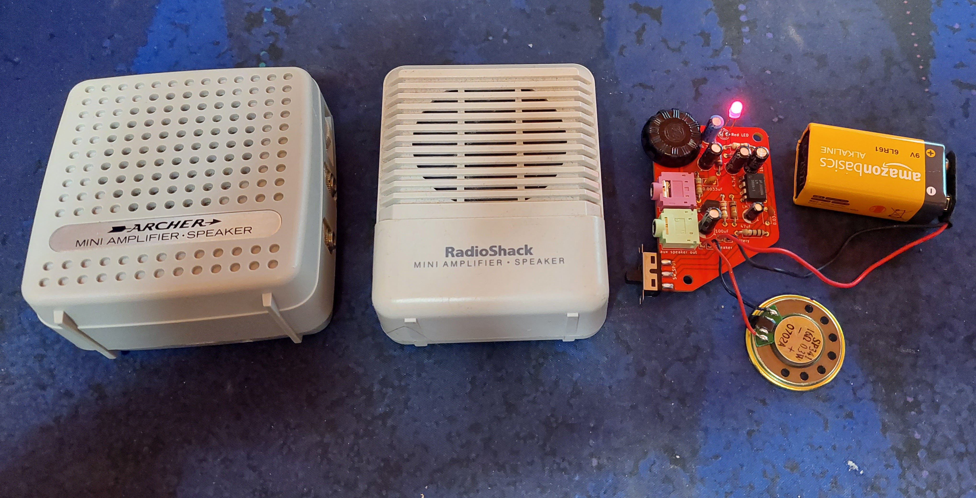
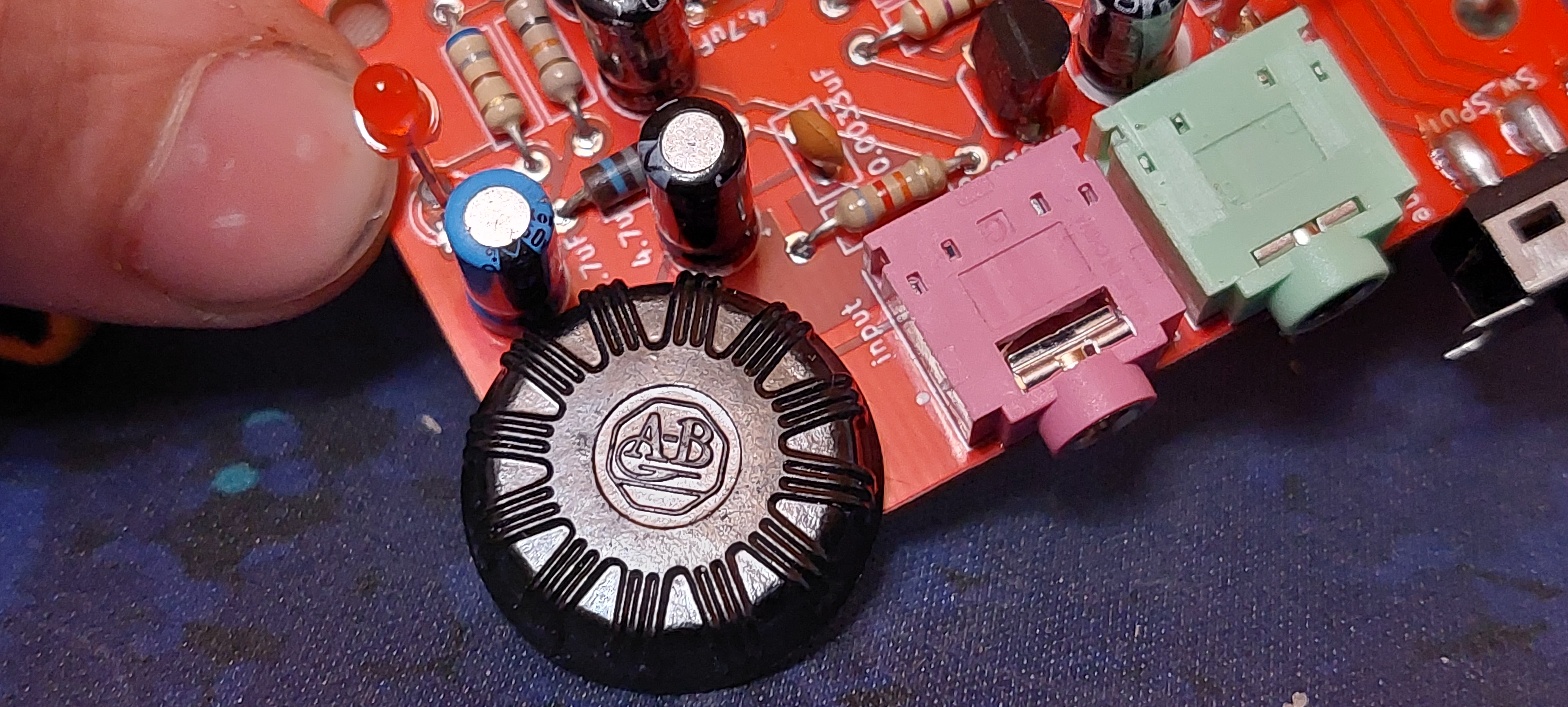
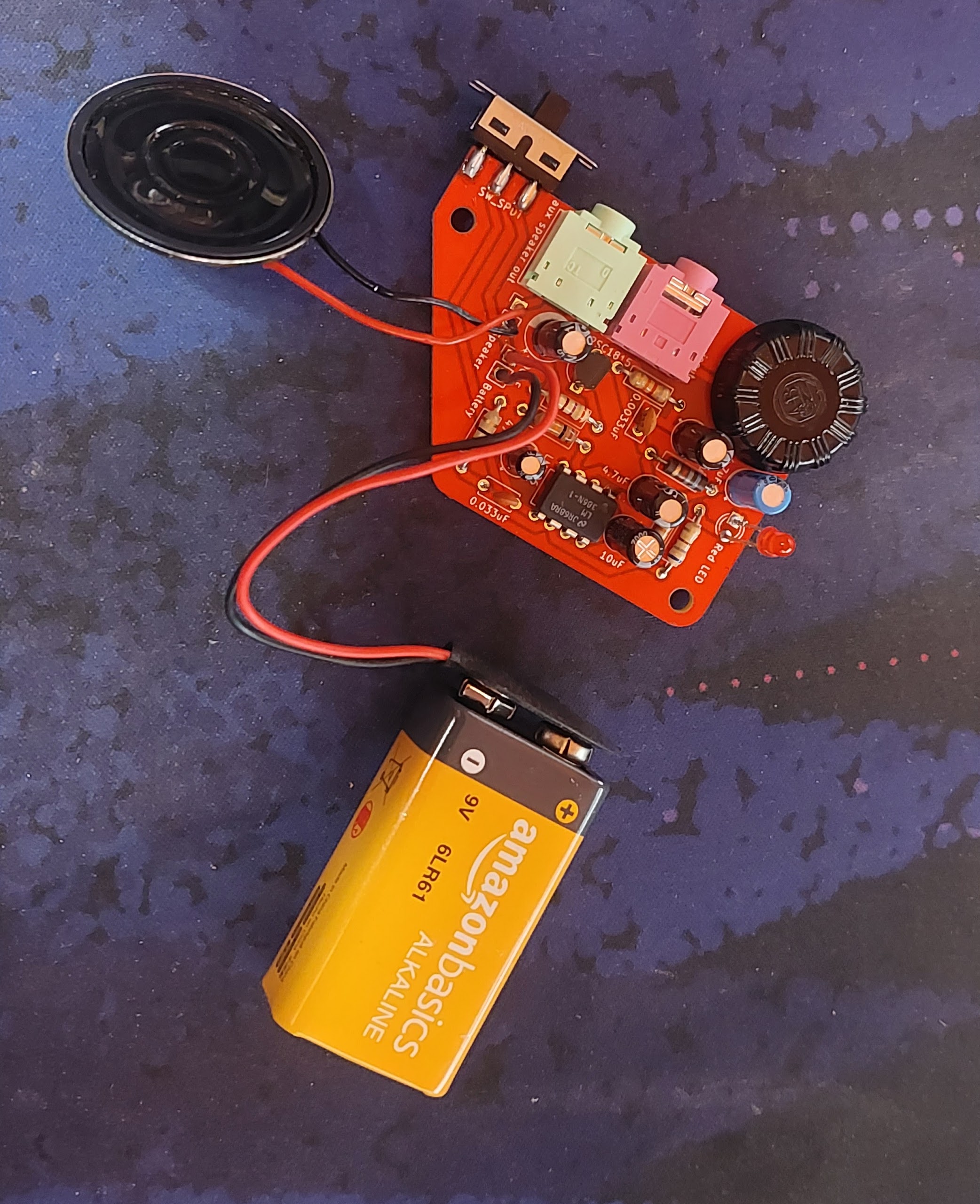
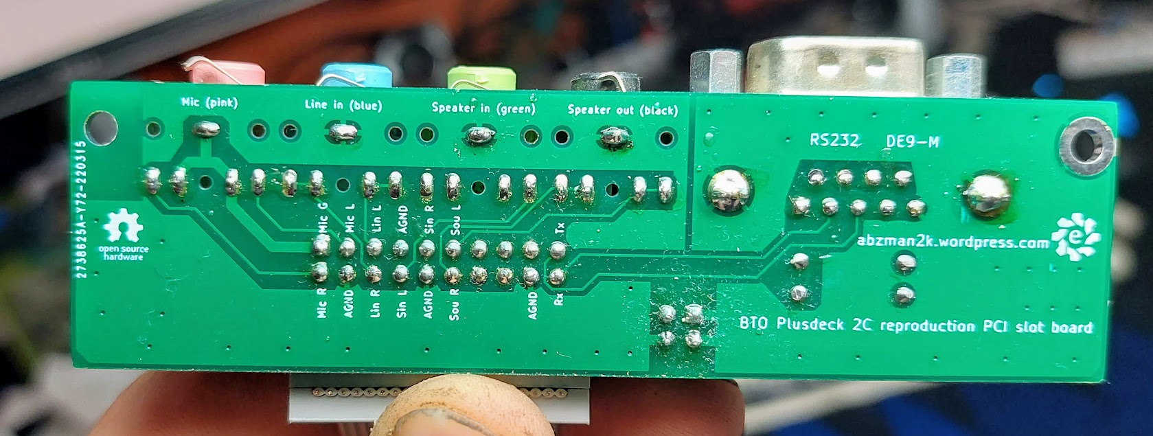
I’ve taken a liking to this small, simple speaker and when I went to go recommend it to someone as a diagnostics tool I found that you can’t get it anymore. Not retail anyway. This is my attempt to make a work-alike version and maybe eventually it will get cleaned up into a version that can be ‘mass’ produced for anyone that wants one. I don’t have this up on PCBWay to order mostly because I designed it around parts in my junk drawer, but I will send you one if you want. I consider this an actually useful bit of test equipment. If you want to know what sound a device you’re fixing is trying to make, this works quickly. If you’re trying to diagnose an audio circuit like an amplifier you can use this like an oscilloscope and follow the signal through the device by listening. You just have to take a headphone cable, split one end, and poke the circuit with the input signal end while grounding the ground pin, and you can follow the signal until it foes away and then you may have the problem component. I found bad slide pots this way in a mixing deck once.
On the left you can see the Archer 277-1008B speaker, in the middle the more modern Radio shack version, and then there’s mine. The original one snaps together and I cribbed my schematic almost entirely from that one, but I made my own changes to fit the parts I had and the features I wish the original had. The Radio shack one has one screw holding it together and a barrel jack for external power if you want. It also has a note calling out that it is center positive as a previous version was not (bad move, but good for fixing it). Mine has a number of alterations and I think it is somewhat improved.
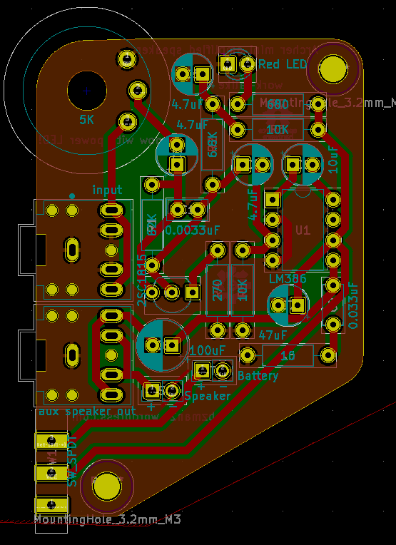
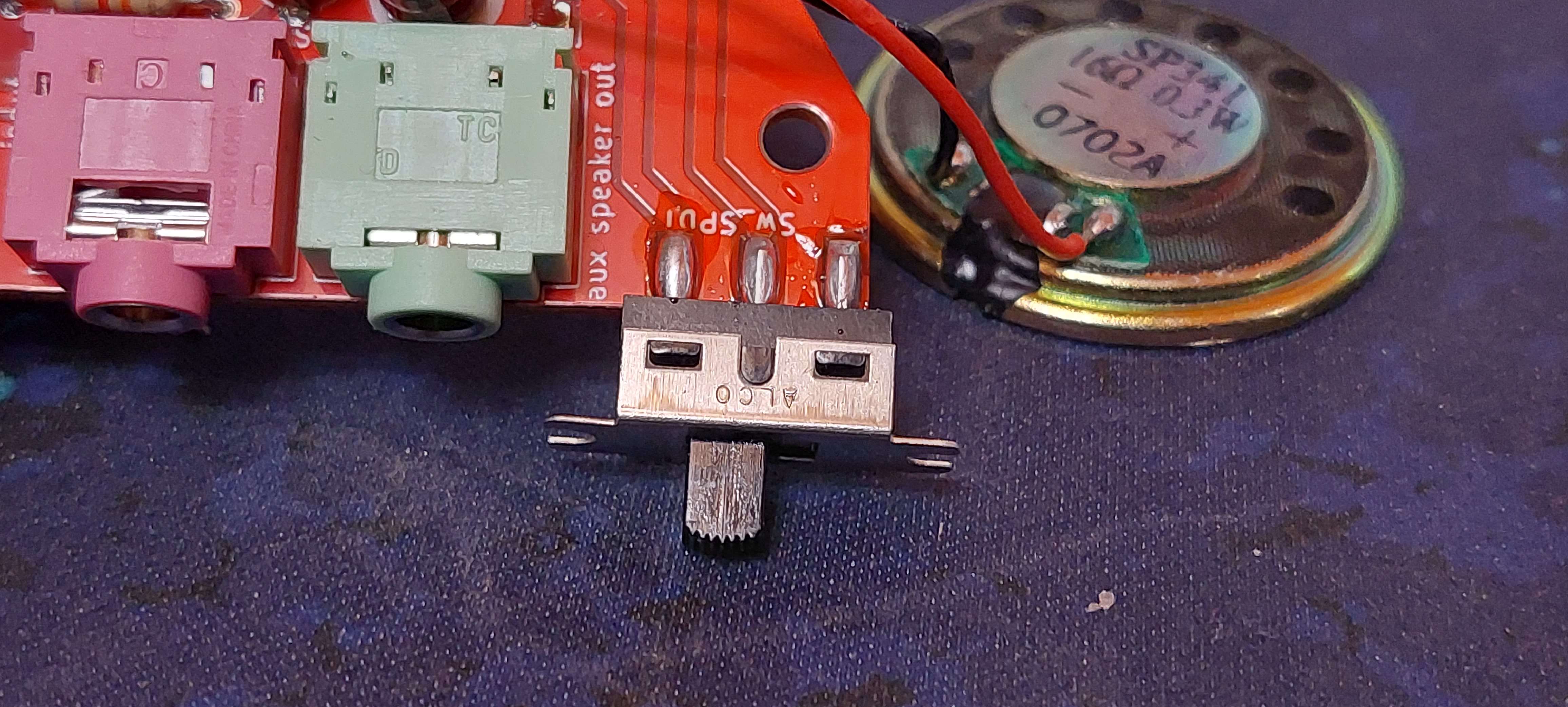
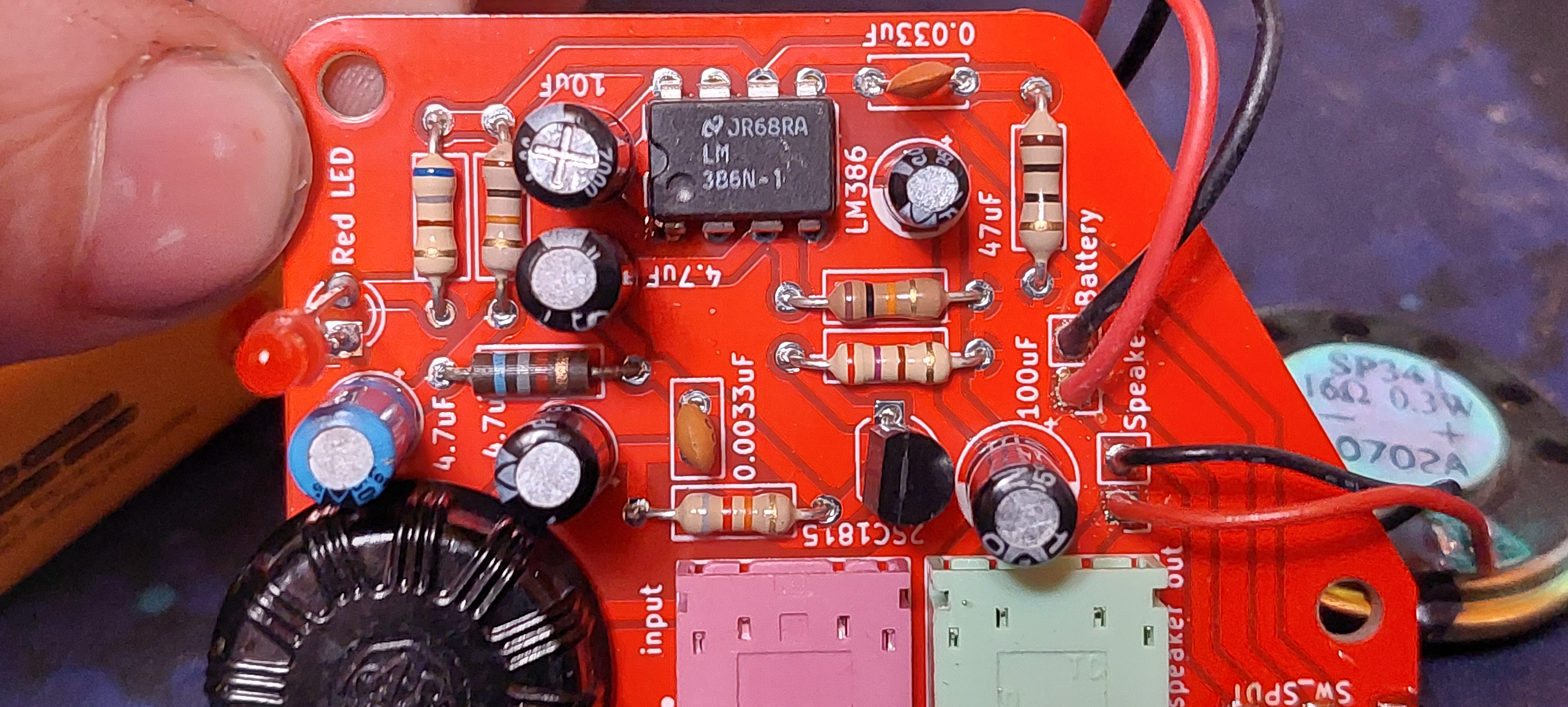
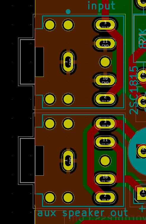
As for the schematic I did a couple things. First I added a power indicator, these speakers will kill batteries if left on and there’s just no way to know if it’s on without twiddling the knob and listening for the crackle. Second I added a switch, the volume pots I had didn’t have a built in switch and I found some switches in a bin that I could use up on this project. The volume pot is actually something I designed a footprint for specifically because I have a ton of them and they’re all identical and I wanted an excuse to use them on something. They’re Allen Bradley parts salvaged by an old Ham that I knew at a previous job. The last thing I did was to use the audio pass-through on the output jack so that when you plugged in headphones the speaker was disabled. This did not work initially, but all the versions built after that used the proper jacks.
The board is an interesting design, I made it as compact as possible while still incorporating mounting holes and all the ports on one side. I could have gone with some surface mount parts but do you know how many 10k through hole resistors I have? They have to go somewhere.
Something I didn’t realize until right now is that I managed to keep all the traces on one side and except ground. I also kept all the traces as thick as I could so there’s be no tearing them off the board when reworking it.
This project did serve as a way for me to use some of these parts. Just look at them, they’re fantastic. These potentiometers aren’t actually the 5K that the original circuit called for, they’re 100K which means that this version has less impedance applied to the circuit it connects to so it will pass more noise. The pot is used as a simple voltage divider though so the range is unaffected in this application.
These switches are also something I’m trying to use up. I have so many parts with a little variance that I’m storing in so many little drawers that I really want to cut down on storing them all. If I can manage to use them in projects, then I don’t have to keep them around. I have used several different switches on the 5 boards I built up and this one is curious. You’d expect because it’s a slider switch that in this position it’s ‘on’. It’s not. The guts of this switch resemble those of a toggle switch where the contacts joined are the ones the lever is *not* pointing at. I have regular toggles too, but this one is backwards. I’m glad I’m using them up.
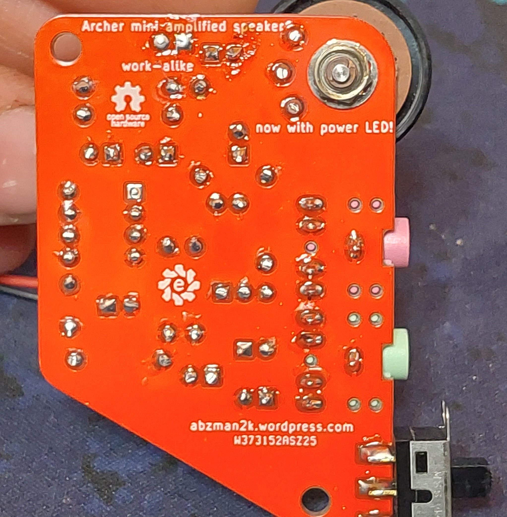
You may have also noticed that his board is in stylish red silkscreen. I figured this time I’d try out something else from PCBWay since they offered to sponsor this project. I already knew they could do the silkscreen crisp and small, but now I can see how well the white silk shows up on red boards. I think it works pretty well, and if you want something to stand out in a clear case this will certainly do it. Getting boards made from these guys is such a labor saver when it comes to clearing up my parts at home. With code the temptation is to try to write it so you can re-use it forever. With PCBs it used to be such a burden to get boards made professionally that you had to get it right on the first try and they had to work in batches of thousands. I can confidently say if you have 5 of one obscure part and you want to put it to use: design a board. Get it made. Solder the parts in. You are done. You don’t have to spend time drilling, or filing, or whittling with a craft knife to make some strange part fit proto-board. measure it with a $20 pair of calipers, draw it up, and have PCBWay build you a bespoke kit of your very own (parts only included if you ask).
Everything on this board is salvaged, the speakers and switches mean that I’ll have to design and print bespoke enclosures for each one of these. There’s no way this design is just ready to order, but when I get my bed adhesion problem fixed I’ll get some enclosures made and four lucky people can get one of these projects for themselves. If you want to play around with the design it is up on my github, but I do not recommend you just have the gerbers made because I cannot tell you where to find one of those potentiometers aside from my junk drawer. I do genuinely think this is a useful design and I expect that for a reasonable price it could be test equipment people would want, just not 1000 of this particular revision.
I fucked up. One of my latest projects did not immediately work and it’s for the dumbest reason. This also has implications on past projects too, so buckle in.
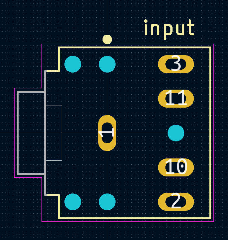
This project will be featured next, but the important thing right now is that it uses a headphone jack. I have a preferred headphone jack that I like to use, a standard footprint that lets me use both salvaged and new parts. This also has some cool features.
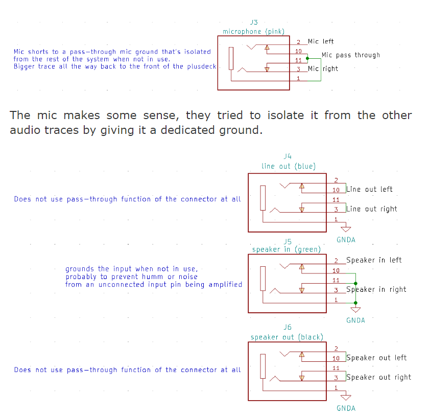
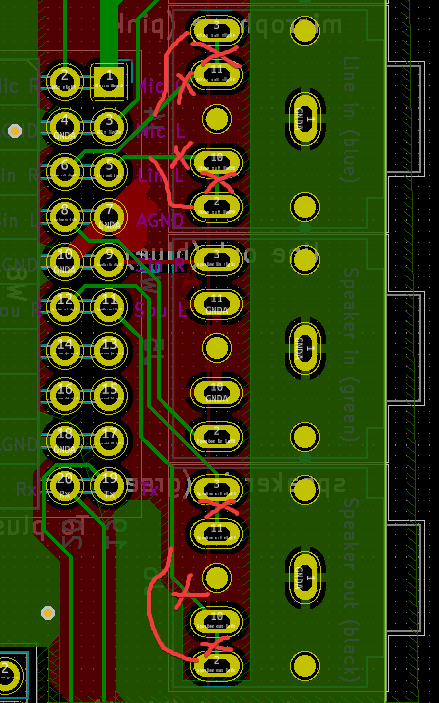
This is the footprint I mean. You have probably seen it around but you may never have wondered what those 5 pins are doing there. The plug that goes in here only has 3 wires so why 5? Well, I’ll show you
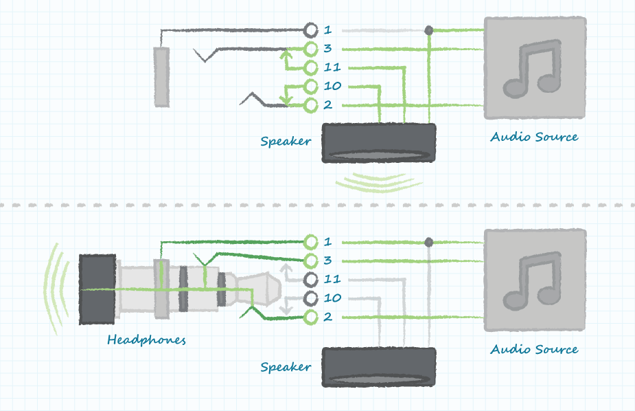
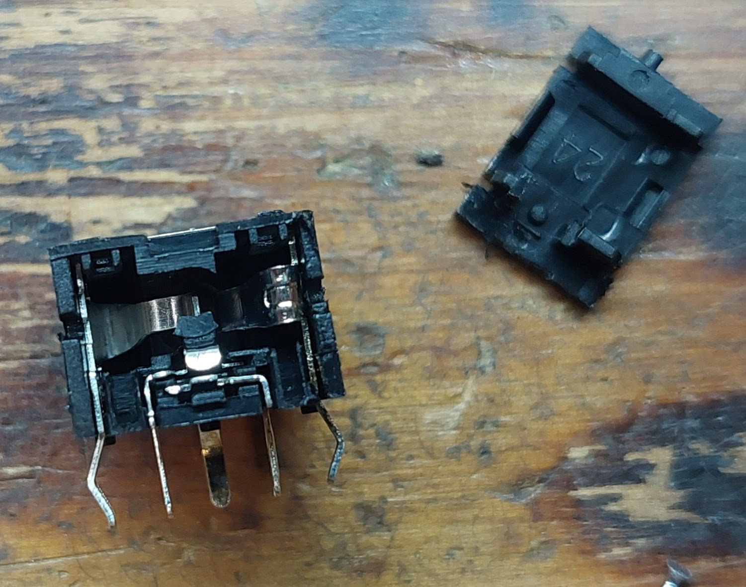
This is what they do, there’s a left and right channel and also pass-through pins that are connected when the plug is not inserted. You can see from this picture that it is frequently used to disable the internal speaker when an external one is plugged in. When my device didn’t do what I suspected I measured the pins on the board and I did not see those pins connected when no plug was inserted. I opened up one of these jacks and this is what I was.
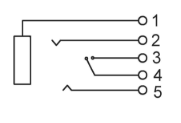
Uhhh…. not good. I think I know what that is, but let’s examine the datasheet real quick.
Yeah, that is an electrically isolated switch that connects when a plug is inserted. Useful, but unexpected. Why did I get nothing out of the speaker?
Well, it’s because I fed the audio out the right pins, but the speaker was just connected to the switch which I thought was a pass-through. This one doesn’t get the ‘mute speaker if jack plugged in’ feature, but I jumpered over the pins so now it does both. The jacks pictured at the top are ones I bought from digikey that do act how I expect. The ones from LCSC have this strange configuration that fits the standard footprint, but behaves entirely differently. What other implications does this have?
This is not the first time I’ve used those headphone jacks. And I even shipped them out to people after I tested them (working I thought!). What are the implications of using those on this design?
The microphone input is not grounded when not in use, it may have some static on it. Not the end of the world. Same with the speaker in connection, noisy but OK. The line out and speaker out though, We have an issue! In both cases when you plug a cable in it closes the switch and makes the audio output mono. That’s not good. Can it be fixed?
Yeah, but it’s not pretty. I’m really not happy about this turn of events and I’ll be using these parts up on things that don’t use the pass through function and never ordering them again. The datasheets were right, they were just unexpectedly laid out.
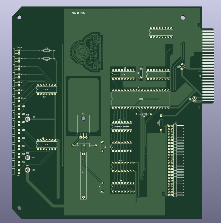
The last board variant I have done is the 0021 lights board. Architecturally this is very similar to the character board, but even from the earliest variant this board never had audio functionality. That means the designers used all 16 outputs from the PIA on this card to drive 24v controlled lights.
The lion’s share of 0021 rev.a is shared with the character card, in fact even the chip locations are shared with 0004 rev.b. If you look at the two unused chip locations on this board, they used to be populated on the character card. The upper one does not have power to it because it was originally an op-amp chip and did not have power on the diagonal opposite pins. The power that did run there was 12v and -12v and that is now gone.
This is the modification for this card to give it 16 outputs. We now use two of the open collector outputs from the 7406 instead of adding another uln2003. That means these outputs are not as powerful, but I think the lights were relay controlled so in this case the high current is not as needed.
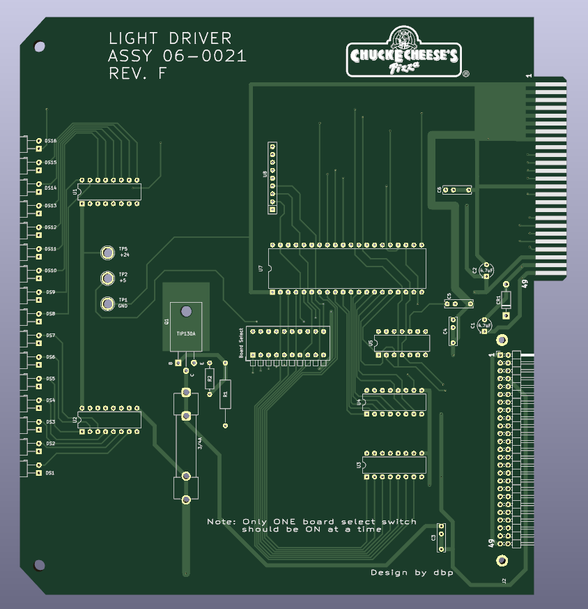
The final board is 0021 rev.f, and I think that naming is probably misleading. This board is part of the post-1993 redesign so it is based off the 0034 rev.e. I think these boards were designed at the same time because 0034 rev.e changes the DIP resistor packs to be 7 resistors per for LEDs and then those two remaining resistors are used on 0021 rev.f. This board includes all the changes from 0034 rev.e except it removes the jumpers for 5v/24v. These boards were never used to drive something like the A/V switcher, so that’s not needed.
That’s it for all the boards I have re-made in KiCAD. If you want a lights board there is no functional difference between rev.a and rev.f. They both have the same electrical interface, they fit the same connector, and all software that talks to one talks to the other. I have the boards up here on github, but feel free to ask me about any issues you may have with one of these setups. I may know something after digging so deep into all this.
There is a whole whack of these, but there aren’t a ton of changes from one to the next so I’ll go over all the details with the first one, then I’ll only go over the differences from board to board.
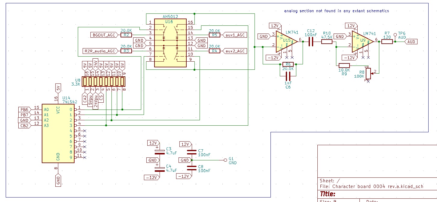
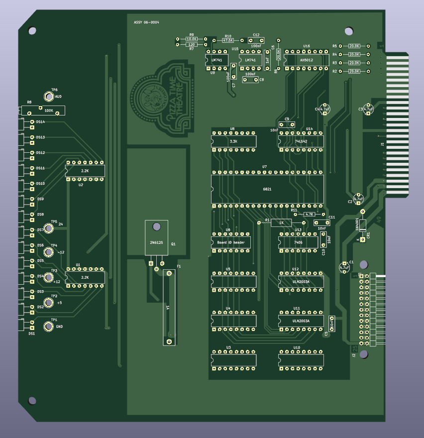
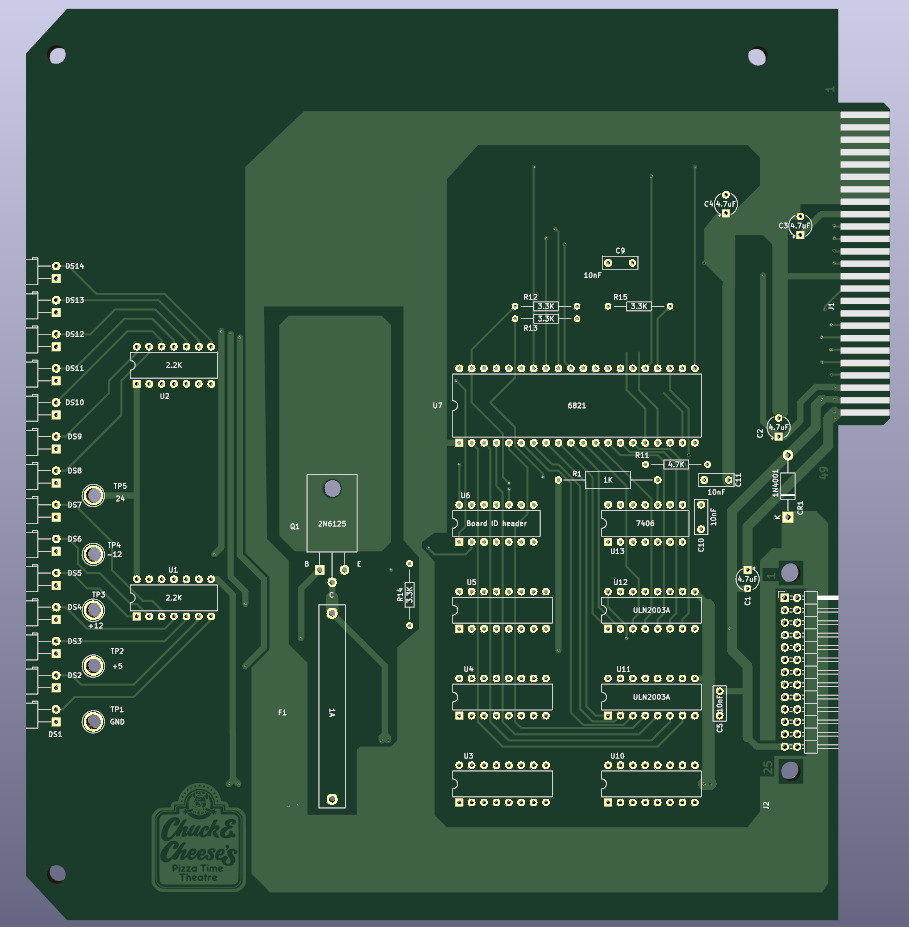
This is the rev.a character board 0004. The only difference between this one and all subsequent boards is this one is about 19mm longer than all the rest. It will fit in the card cage, but it will stick out a bit. The board layout is kind of interesting in that it includes a lot of empty IC sockets for potential bodges that may be needed. Let’s look at the schematic one bit at a time.
On the left we have power coming in and the board ID header. This lets you connect the chip select for the 6821 PIA to one of 10 pins on the card edge so it can be uniquely selected by the CPU card. If you really wanted to you could set two cards the same and have them mirror their movements, but I can’t think of a practical use for that. Then we have CA2 controlling the ‘high’ voltage. It switches the 24v supply out to the character ribbon cable to control all the solenoids out on the character. At the bottom right we have the returns from the solenoids and each can be grounded to complete the circuit for the solenoid. These are tied to LEDs so you can see what movements are being commanded to the animatronics. If the fuse blows these LEDs and the solenoids will not function. This card has 14 outputs, but that’s for a good reason.
This is the audio section that is only present on the 0004 character cards (I have seen rev.a and rev.b). This works with the 0003 audio card to choose one of four audio tracks to play. I know it only chooses one because it uses a 74ls42 to pick and that chip has mutually exclusive outputs. In this case the remaining 2 bits of the PIA are being used to pick which track, and CB2 is being used to enable audio at all. Once the track is selected (I suspect it’s 3 tracks from a reel to reel and one for mirroring the background game room audio) it gets amplified and volume controlled before exiting the card onto pin 2 of the character connector.
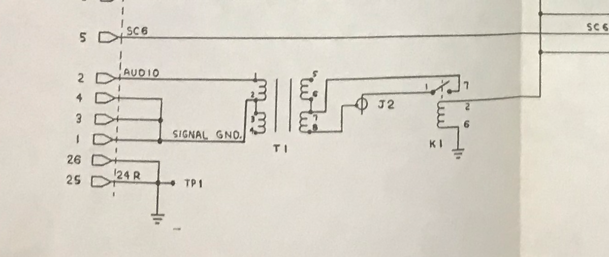
This is the circuit on the solenoid driver card. It seems to be a matching, or isolation transformer and a relay controlled by the 24v line to the solenoid card. I don’t know if there was supposed to be an amplifier at the character, or it was just a speaker coil, but this is how these characters worked. If you have the more modern 0033 audio card this output would still work because two of the four channels are still available to be chosen from (one being the reel to reel, the other being the background audio). The ROM that’s driving your unit just had to control the audio on the character card, which the one that we have disassembled does.
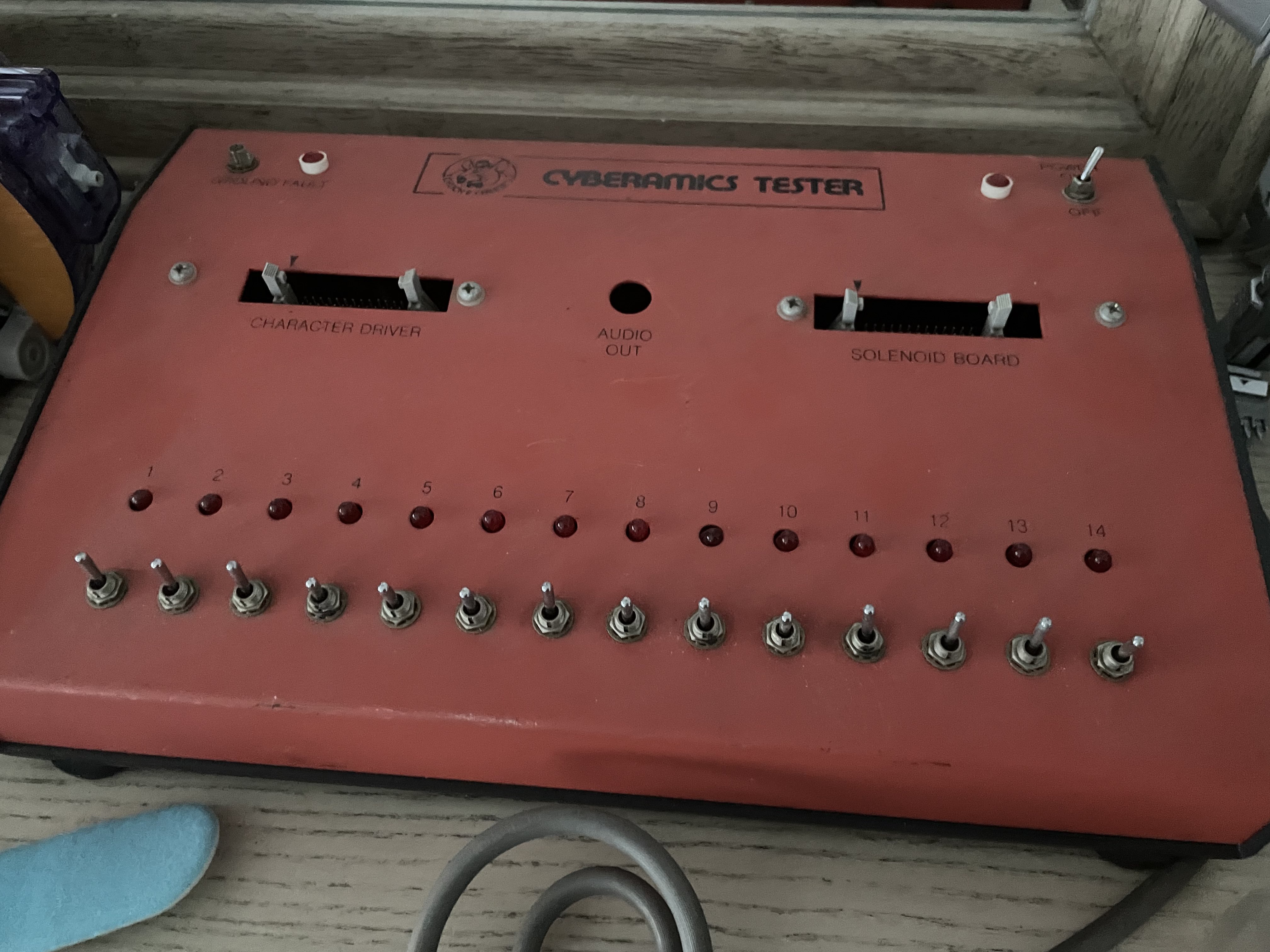
This cyberamic tester now makes more sense. It seems to sit between the computer and the animatronic to indicate what solenoids are trying to energize, over-riding them, and also having an output for the audio signal.
0004 rev.b really just changed the board length. There’s nothing else of note, but this is the standard board size going forward.
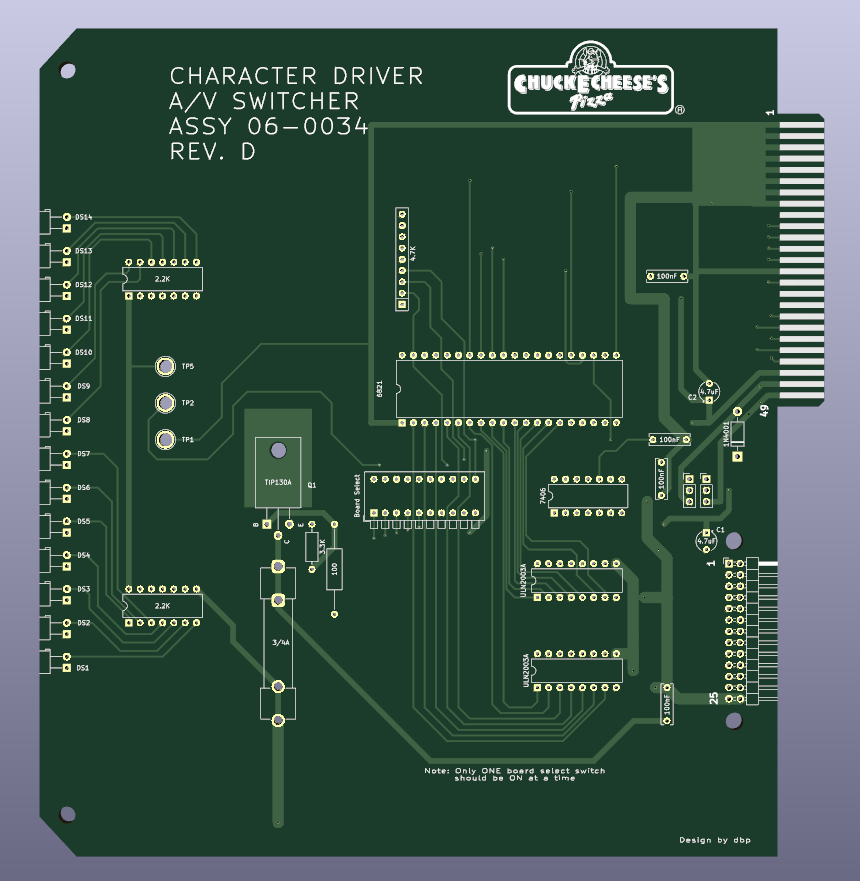
0034 rev.a dropped the analog portion. It does not re-use the outputs controlling it however, so if you want to run the same code that twiddles those bits that is perfectly safe, it just does not do anything. They updated the logo to this square one, and removed one DIP resistor pack in favor of individual resistors as there are less than a full pack being used with the audio stuff gone. The 12v and -12v stuff from the audio stuff still exists, but it just has capacitors and test points on this board, neither of which are needed for this card’s functionality. This card is intended to pair with 0033 audio cards because those do not need the character cards to handle the audio, but as stated above they still can, but for 2-channel functionality instead of 4).
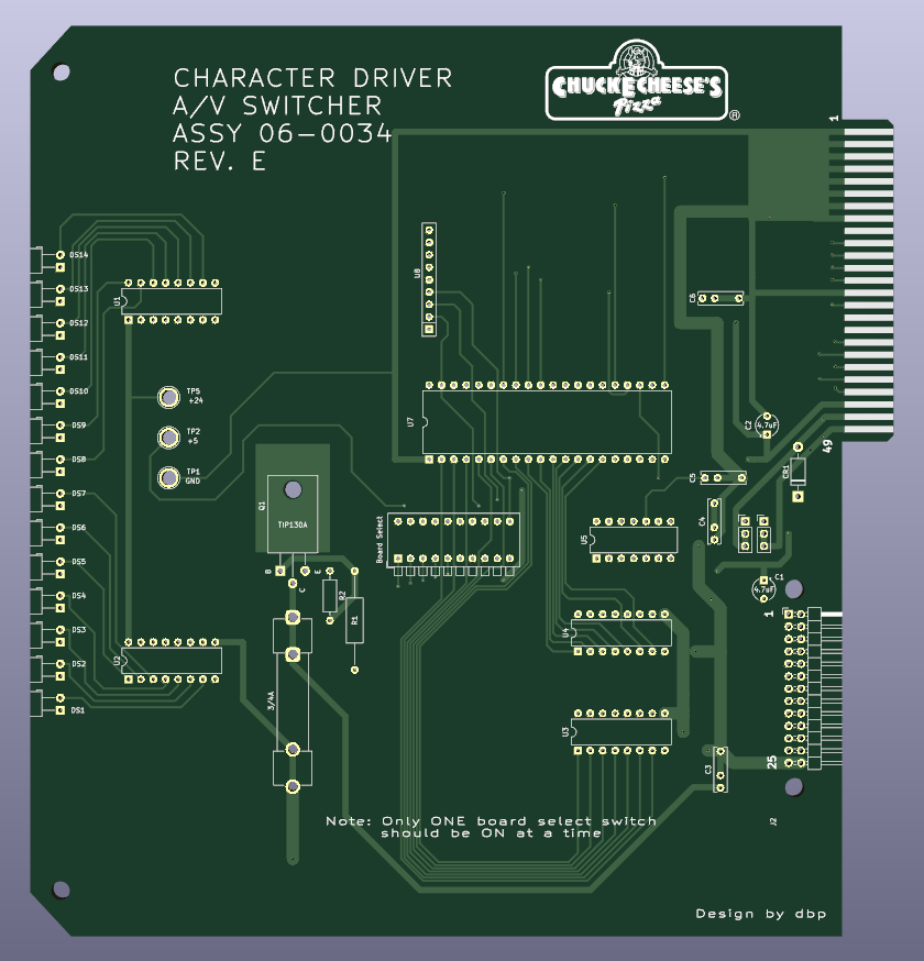
0034 rev.d is a major overhaul and the first post-1993 board I’ve done a reproduction of. There are a bunch of changes, but largely not to the functionality. The solder-in fuse has been replaced with a fuse holder, the transistor was changed to a more modern TIP130A, and the spare chip locations are gone. All the 12v and -12v stuff is gone because this board doesn’t really share that same heritage and got a big facelift. The main chip is the same, but the IC socket with jumper packs to select only one board ID is replaced with a set of dip switches with a stern warning to only select one at a time. That is because the chip driving all those chip selects is a 74LS42 which drives one output low and all the other outputs high. Selecting multiple IDs at once would connect 5v and ground together and that wouldn’t be good. The other major change is a set of jumpers that you can connect to make he output voltage 24v or 5v. This is because the character cards from this generation were re-used as general purpose output pins to control an external A/V switcher. This generation did not use the audio card at all. Those resistors that were split off before are now back together in a SIP resistor pack. There is also a new logo, but this time it’s on the silkscreen.
The last character card I have seen is the 0034 rev.e board. There are only minimal changes from the last one. The capacitors are now multi-footprint so you can populate them with two different pin-spacing parts depending on what you have. The 24v/5v jumpers now have a default position of 25v and you have to cut the copper to get a 5v board. The silk now has different reference designators, and the underlying references may have changed in the last revision but the silk had values there and not the references. There’s also a sort of unexplained track re-routing. These tracks seem to dart around some non-existent chips, and since I know what the immediate previous version was, I have to assume this was maybe to add some other function but it was dropped.
That’s it, that’s all there is for the character cards. I have versions of all of these up on github, but there’s really only two you might want. If you need audio functionality, use 0004 rev.b as it’s the right length. If you do not need audio functionality and you want the modern amenities go with 0034 rev.d. I’m not sure how I feel about dip switches, if you don’t realize which way is ‘on’ you may accidentally short it out. I will be continuing to explain the subsystems and functionality of the cyberamic control system in upcoming posts (I think I only have one more). Feel free to ask me about any issues you may have with one of these setups. I may know something after digging so deep into all this.
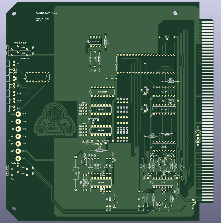
The third board I’m going to try to explain is the audio board. This one was harder to do than the others because even though the transport board had an incorrect and incomplete schematic, this board had no schematics. That means I had to put together these replicas based on a bunch of reasonably good pictures, some measurements done at the museum who let us have some time with the cards, the disassembled code, and the other cards for reference. This ends up being a big puzzle figuring out where all the connections go, and sometimes it takes some looking at the datasheets for the parts and saying ‘well, this has to be pulled high otherwise it would never work’ and just rolling with it.
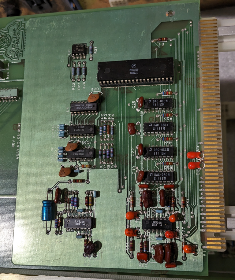
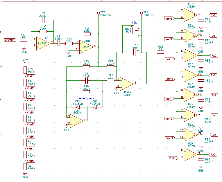
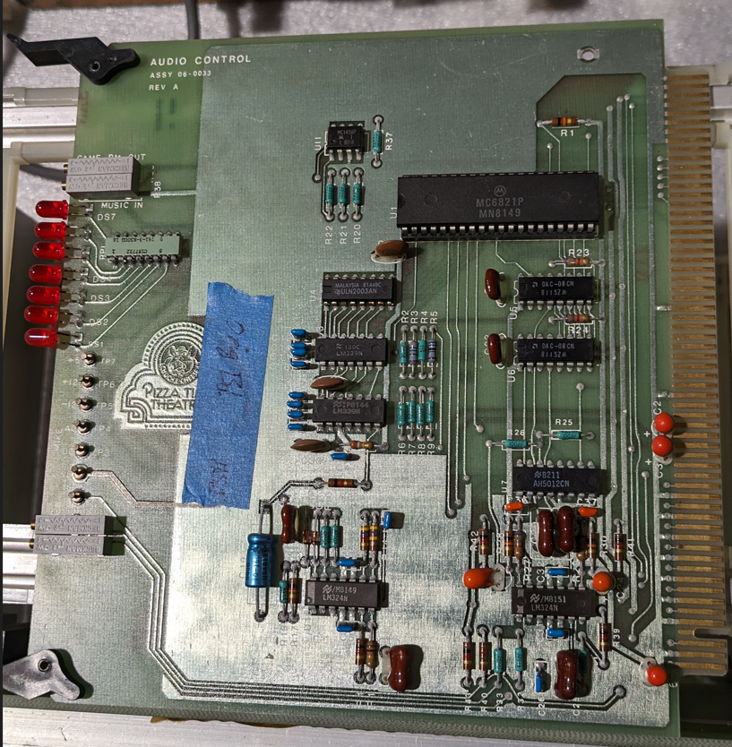
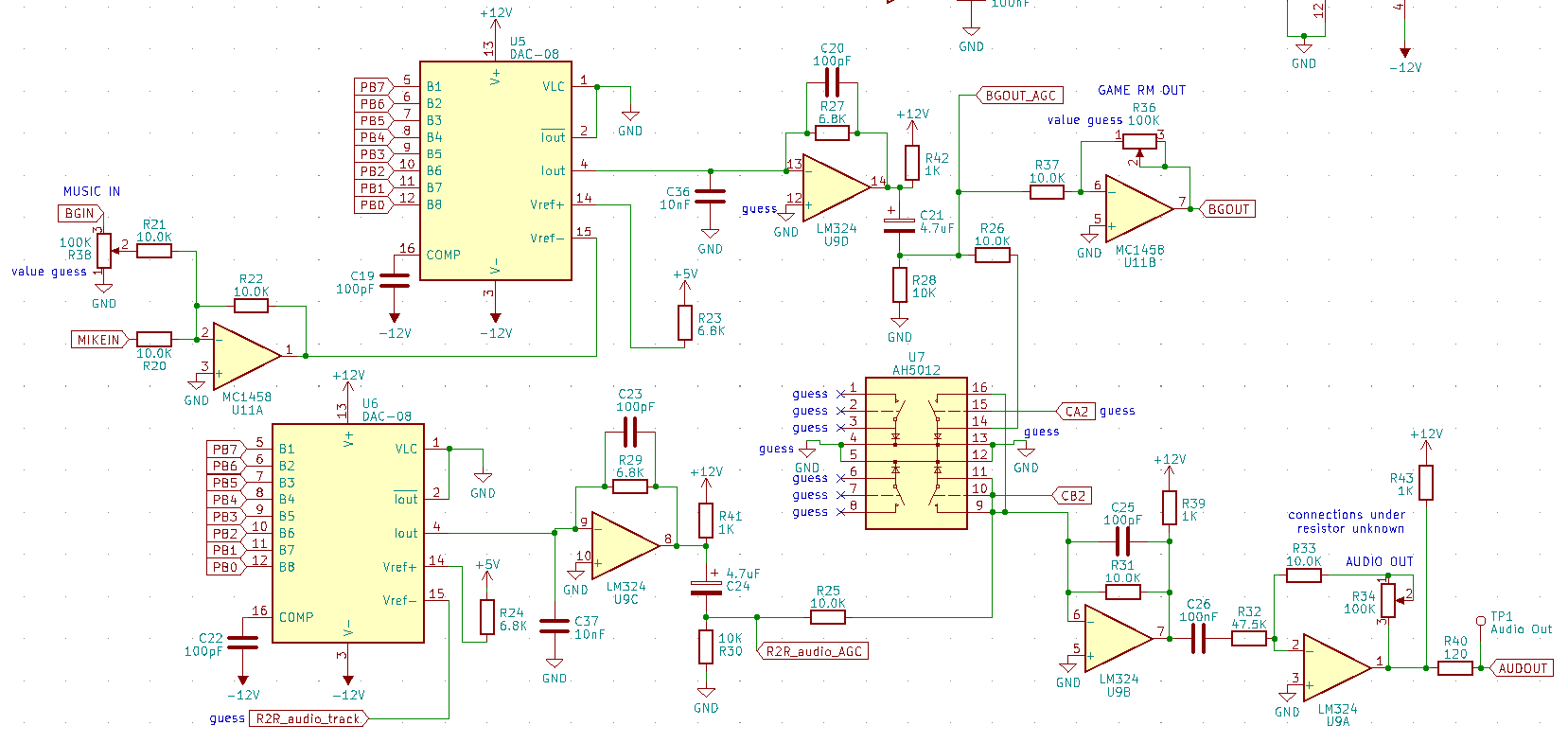
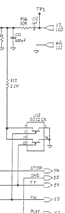
The first card I want to talk about is the 06-0003 rev.c board. I only have rev.c of this board, but it is clearly the earlier board. It has two main functions, measuring the room audio level, and controlling the volume of all the audio channels. We’ll start with the first part.
This is the automatic gain control microphone input. I don’t know exactly what all the filtering is doing but I know the main thrust of what’s happening. The room audio is picked up, amplified, filtered in what I assume is an envelope circuit to get a nice smooth analog value for the average room volume. That audio is fed into 8 comparators that compare the analog room audio level to a set of fixed voltage offsets coming from that large resistor ladder with many taps. This produces one of 9 states, either the audio level is below the first comparator, or it is at or above the level of any of the comparators in the chain. This is not a binary counter sort of situation, if it is halfway up the possible volumes then the bottom 4 comparators are all detecting it.
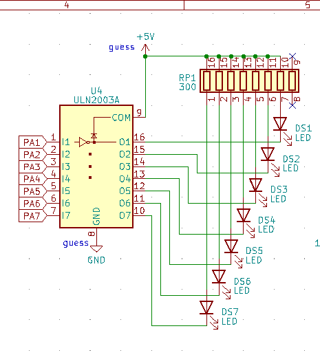
The 7 most significant bits of this are put directly on the LEDs on the front of the card. Even with no CPU installed, this circuitry will detect the room audio and present it on the LEDs. That data is then fed to the onboard 6821 PIA chip so the state can be read by the CPU. Once the CPU decides what to do with the audio streams based on the ambient audio level and the automatic gain control knob on the front panel (or a possibly just a table lookup in some versions) it commands the DAC chips to control the audio levels.
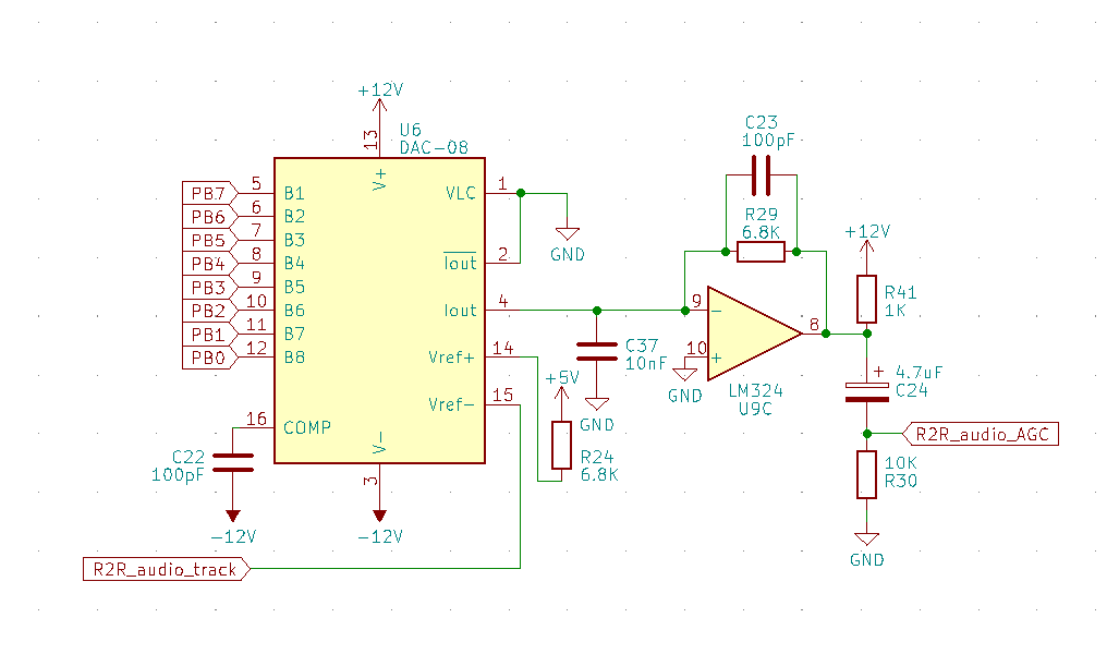
There are four sections on this card that look identical to this. This operates in an… interesting way. I would expect a digital to analog converter to take a purely digital signal and reproduce it between a high and a low fixed threshold. That is not what this does. One of the threshold pins is fed analog audio and the output is that audio, but gain controlled to 256 possible levels. I suppose you can use a DAC with external Vref pins as a fancy volume control, but I didn’t expect that. I said there are 4 of these circuits, so that means 4 input pins for 4 analog audio sources and 4 pins on the card edge connector to put the 4 gain controlled audio signals. There is one slightly different channel though.
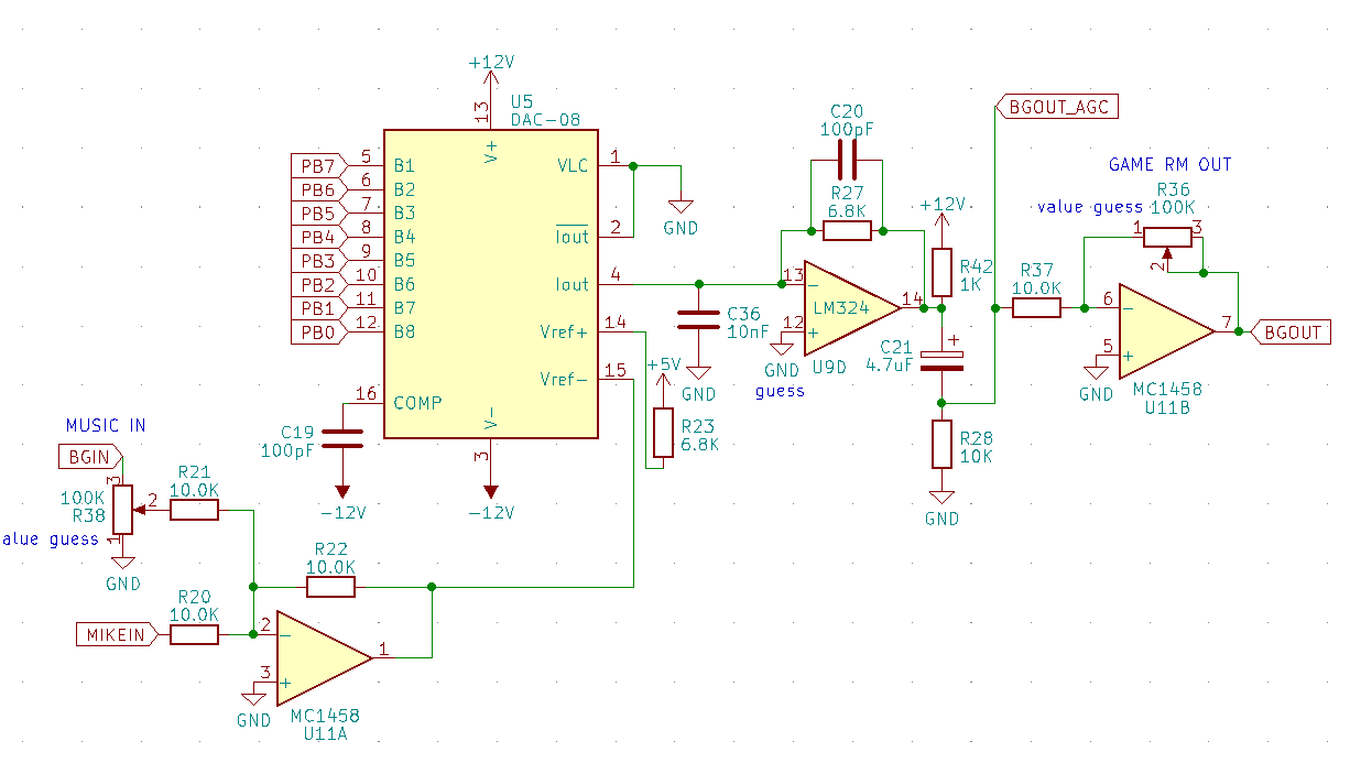
This one takes the background audio (game room music) in with its own volume pot to set the relative level. It mixes it with the microphone input, not the AGC mic, but the microphone where an employee might make announcements. That audio then passes through the same amplification stage as the rest, including going out to one of 4 pins on the bus for gain controlled audio. This stream just also passes through another amplification stage with its own volume control pot and goes out a separate output dedicated for the background audio. The output here always has the combination of game room audio and microphone going out, it just gets volume controlled by the AGC circuitry.
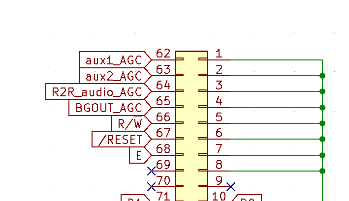
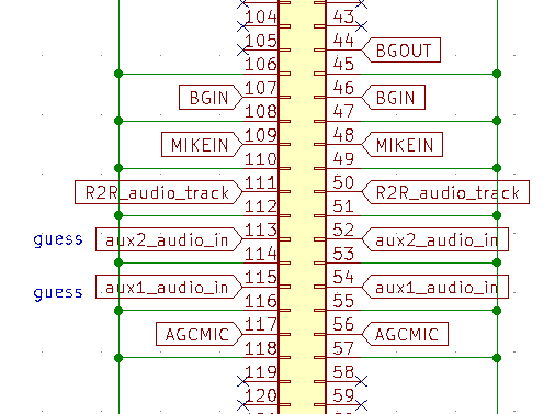
Up at the top of the connector are the 4 channels of audio that go out on the bus, all amplified equally. At the bottom you can see the analog channels in and out. I have only labeled one of them R2R audio meaning reel to reel because the cable setups I have seen only have that pin carrying the audio from the reel to reel show tape. Where do the other channels come from? I don’t know.
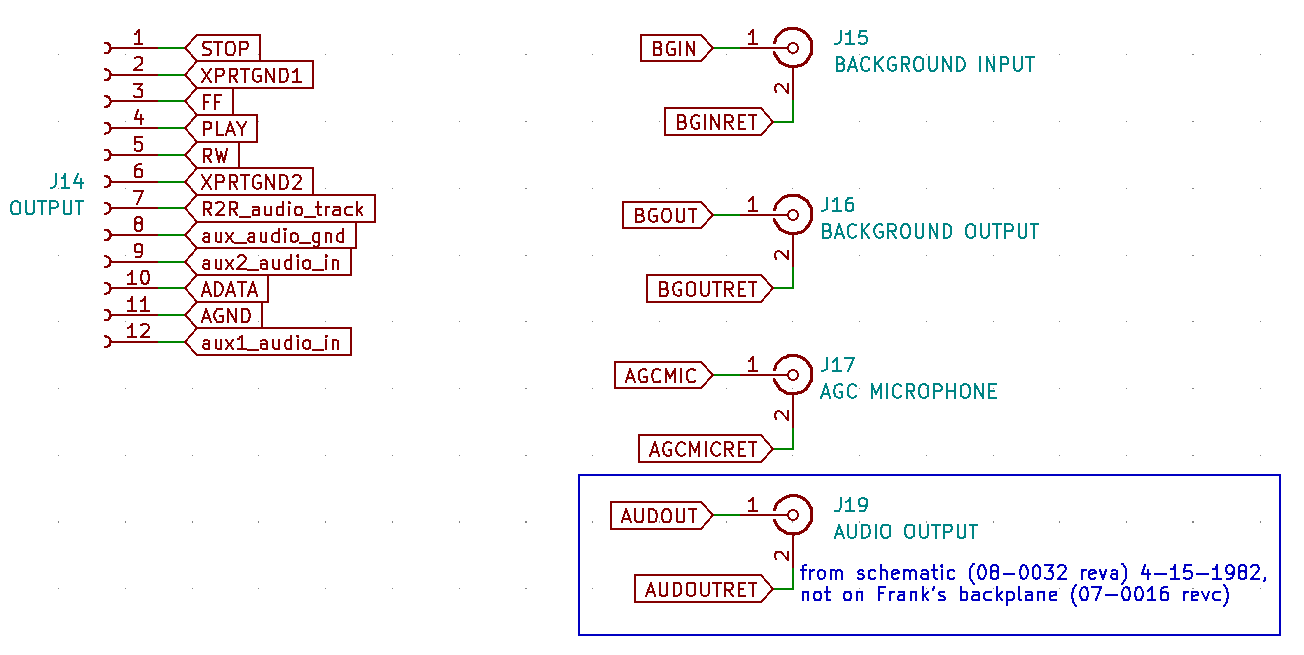
This is that section of the backplane schematic. Ignore J19 for now, this card does not use that. The backplane has 3 RCA connectors for the background audio in and out, the microphone for AGC, and not pictured is the employee announcement microphone that looks like it comes in from the big power supply/button unit. J14 is a big Molex connector that has a cable that goes to the reel to reel machine. On the one in the museum the pins for aux audio are not populated, I only determined that’s what they do from looking at how this card functions. The reel to reel already has two tracks, one for data and one for audio. Was this originally used with a 4-track reel to reel machine with 3 audio tracks that could play in parallel? Maybe, but I’ve never seen documentation that indicates that or tapes with 4 channels of audio. How does the audio get out of this card cage? Well, for this card (0003) you need to pair it with the older character card (0004) and on those cards they decode which of the 4 audio tracks to output and output them locally at the character. I’ll get to that in my next entry.
The next card I have is 0033 rev.a. Note the extra 3 in the tens place, this card is not a predecessor to the last card, it is a successor and is not fully backwards compatible with it. The AGC functionality is the same, but only two of the audio amplification sections are present. Those sections then do this:
If you squint you can see the similarities. The background audio and reel to reel audio sections are the same. At the point they go out on to the card edge connector (which still happens) they are also connected to this analog switch. This switch picks which audio channel will go out the new mixed output. The way it’s wired we could have one or both or neither output, but I suspect they are never both output at once. This means that the single audio output either functions like the room speakers, or it puts out the show audio instead while a show is running. The output stage re-uses the two op-amps from the now missing aux channels and tit has its own volume pot for setting the level. This audio does go out J19 on the backplane.
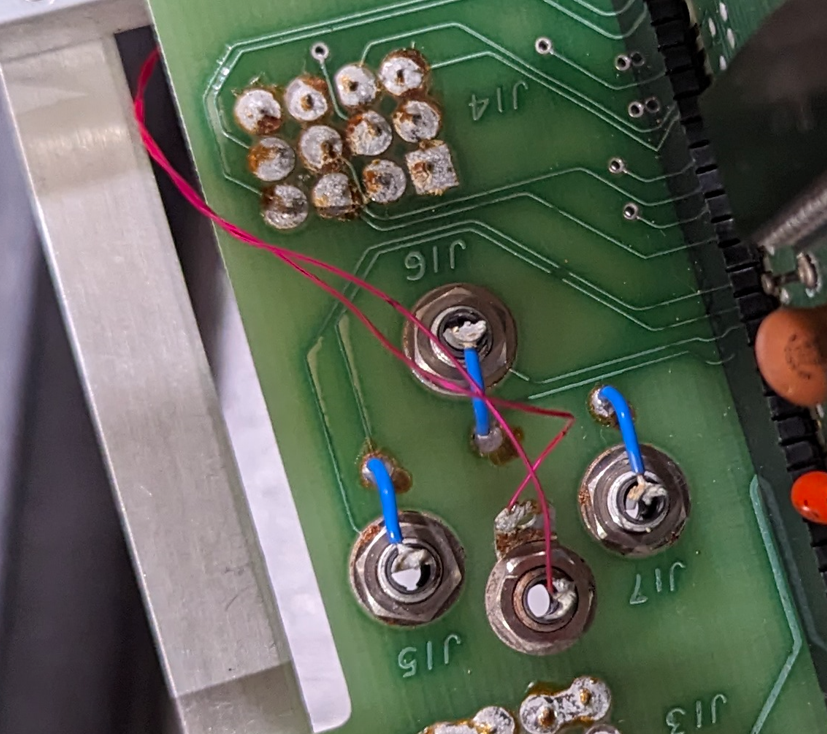
Here’s the thing, I’ve never seen a backplane with J19. It’s always added by hand like this, and this is the third backplane I’ve checked. Clearly the backplane was designed for the 0003 board that didn’t need this and was retrofitted, but were any backplanes produced with J19 installed? the schematic I have has it on there.
There are some routing choices that make it obvious that 0033 came later and was modified to suit. The wires that just chop through the ground plane there at the bottom for one. There’s also some traces on the back of the board that dodge chips no longer present and connections that used to be for the other two analog audio inputs. Here’s some important things to note:
If you have a 0003 audio board
you must use it with 0004 series character cards
the character audio comes out those cards
you are compatible with 4-channel recordings (early?)
If you have a 0033 audio board
you can use any character card
the character audio comes out J19 on the backplane
you are only compatible with two-channel reel-to-reel recordings
The ROMs Frank and I have disassembled have code that controls both the audio switching on the character cards and the audio switching on the audio board. This makes it universal and can work in either setup. The ROMs we have are only for The King configuration, however, so it remains to be seen what additional control is done to handle other character audio.
I think it’s super cool to be able to have the audio come out of the animatronic that’s currently talking, as well as having multiple channels that can talk over/with each other. Apparently this was used for some early setups, but did not stick around as the audio from the characters was not loud enough. As always the cyberamic stuff is all on github here. I will be continuing to explain the subsystems and functionality of the cyberamic control system in upcoming posts. Feel free to ask me about any issues you may have with one of these setups. I may know something after digging so deep into all this.
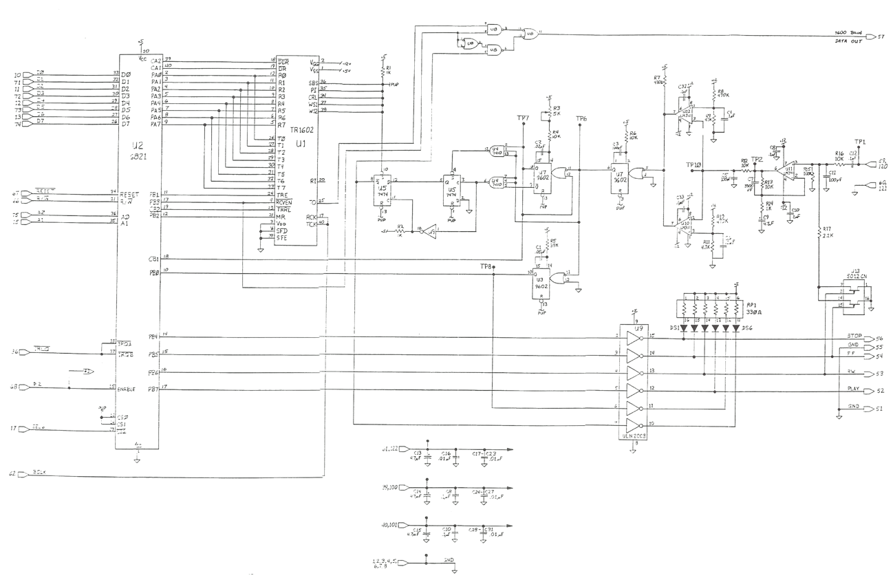
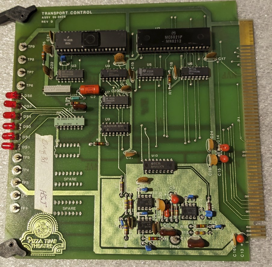
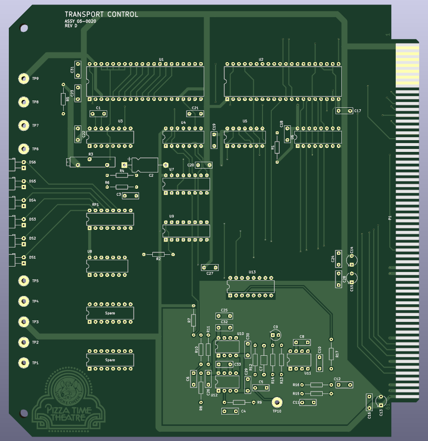
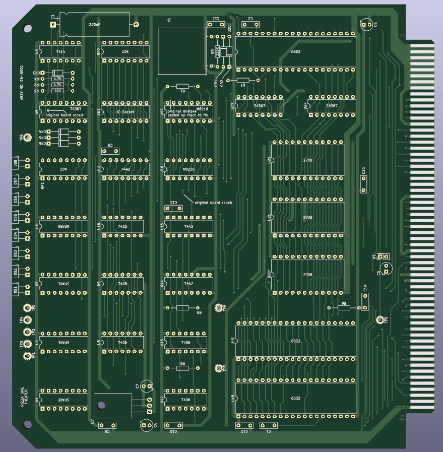
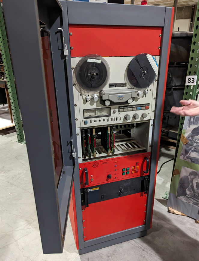
The second board I’m going to talk about in this series is the transport board. This board controls the Teac X-7 reel-to-reel machine and processes the audio from one of the tracks into serial data. This one I have a schematic for, but it’s not for any version that I think existed for real. It has some clues to a version I don’t have and shows a feature of a later revision that I do.
Like most boards other than the processor, this board is based off of a 6821 Parallel Interface Adapter. Connected to that is a TR1602 UART serial chip. Think of this as something similar to your standard 8250 or 8251 that you find in a lot of Z80 designs. That chip is hooked to a whole bunch of analog circuitry that takes audio and turns it into sensible serial data. There are some errors on this schematic though.
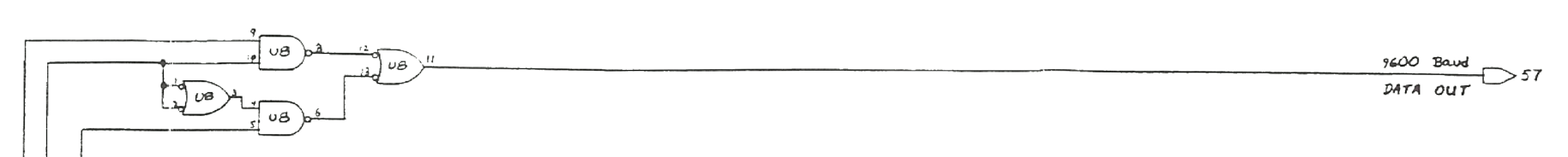
This section at the top of the schematic does not exist on either the revision B or the revision D board that I have seen. It would work to output a serial data stream there, but on the real machine it would only be at 4800 baud. Pin 57 is not used for anything on either of the transport cards I have seen, and it is not hooked up on any backplane I have seen, so it’s possible this was dropped early on in the design.
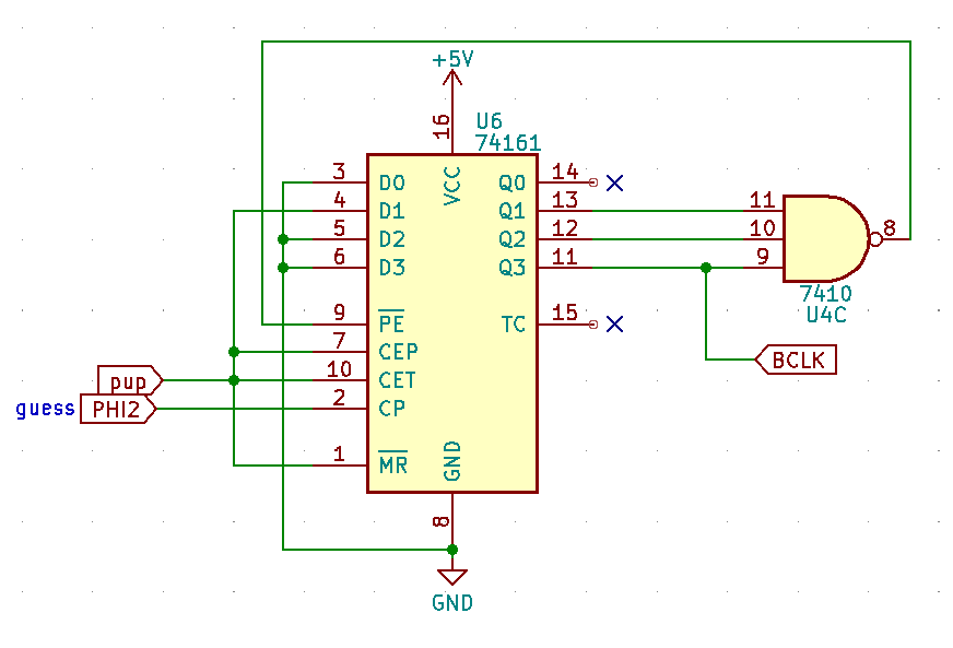
The schematic claims to get the serial clock from an external card edge pin, but the boards I have both use this circuit. I haven’t been able to verify that it is wired exactly like this, but it’s a best guess from pictures and context clues. This is a divide-by-13 counter and that makes the serial clock from the CPU clock. The pin that it claims to get the clock from is used for an auxiliary audio source on some cards I have, so perhaps there was an idea to use this serial port in a synchronous mode where the clock and data are both provided by the same source? I don’t have hardware that would support that other than speculation, and the schematic has no conditioning circuitry to adapt what would have been an analog waveform into a digital clock, but that’s my only guess for why the schematic places the clock input there.
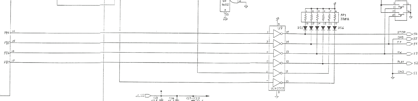
The lights on the front of this card indicate how it’s currently controlling the reel-to-reel machine with the stop, fast forward, rewind, and play functions. There’s also two extra LEDs that indicate if there is a carrier and show the serial data being received.
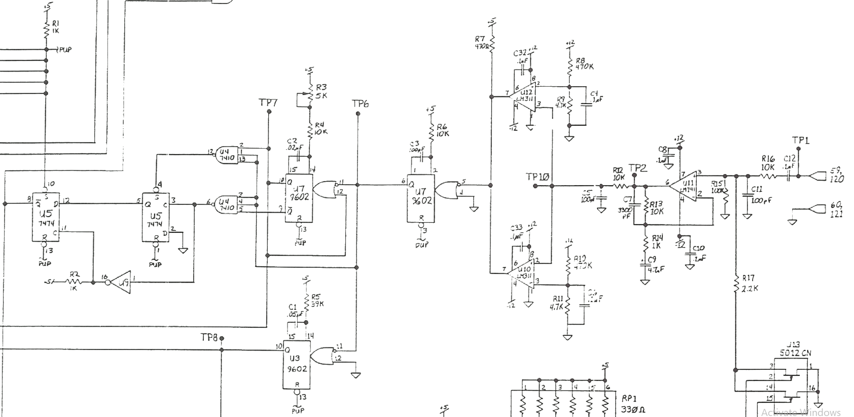
The serial data conversion from the analog waveform I can only speak about in high level terms. From what Frank told me and what I can see here the audio gets filtered, the zero crossings are then detected, some timers similar to 74LS123s generate and detect pulses of the required length for bits of data at 4800 baud, and from that we can see if there is serial data available or even count the zero crossings manually.
There’s also another chip that pulls the audio input volume down if the card is commanding the reel to reel deck to run in fast forward or reverse. That’s pretty odd considering the Teac deck has circuitry to mute the output whenever it is in either of those modes. There’s a clue though, in the bill of materials for constructing one of these systems it asks for the specific reel to reel machine:
What does it mean that the tape deck is ‘modified’? Well, After a discussion between Frank and someone very knowledgeable about these things it turns out that one resistor is shorted in the deck and that disables the muting of audio during fast forward and reverse. But why would they do that? It turns out that there is a low 21 Hz tone encoded between segments of the tape, at least for the tapes meant for ‘The King’ or other single animatronic character shows. These tones are sped up and amplified when the deck is running in fast forward or reverse. The code in the ROM looks for that tone and uses it to determine where it is in the tape (how many shows are left) and when it hits the end it uses that to detect a long pulse at the beginning of the tape so it can stop rewinding. Based on the hardware and the code that frequency can be anywhere between 166Hz and around 3200Hz. A very forgiving range to account for the differences in speed of the rewind and fast forward mechanism.
The real cards aren’t so pristine as this schematic shows. The revision B card doesn’t have that function to lower the volume of the incoming audio. That seems to have been added to account for the fact that the tone on the tape was amplified when it runs fast across the heads. Without it the input amplifiers on the card may be overwhelmed and cause some errors in detecting where to stop the tape
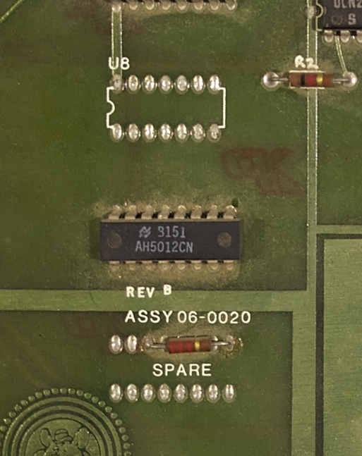
There’s also a spot for a chip labeled U8, but no traces other than power and ground go there. Unused chip locations on these boards are labeled ‘SPARE’ as you can see, U8 looks to be a leftover from when this board put out the serial stream on pin 57 as indicated in the schematic.
Revision D incorporated that chip into the main board design, but it retains the U8 designator. I suspect that chip was on the revision A board but removed after that because nothing else in the system needed the serial data. This board connects the interrupt line to the same pin that the CPU card has, but the backplane doesn’t connect them. If you wanted to you could wire wrap a connection for it, but the tape data speed is slow enough that the CPU doesn’t need an interrupt. Maybe that’s a leftover from the planned 9600 baud?
I have a full replica of both versions of the board. If you’re going to make one I suggest revision D because it contains all the features. If it were me I’d also add a bunch of silkscreen to explain the LED functions and the test points (and the values for the components), but that breaks from the authenticity of the recreation. Thanks to Selena for helping me convert the logo to monochrome in the right way to make this board authentic. This is not the only time I would need that sort of help. If you need one of these board I can make you one, or you can find the design up on github here. I will be continuing to explain the subsystems and functionality of the cyberamic control system in upcoming posts. Feel free to ask me about any issues you may have with one of these setups. I may know something after digging so deep into all this.
I’ve spent the last several weeks staring into my light table and generating board designs. Most of these designs are replicas of designs I have the real boards for. That is mostly for complete-ness and to have the designs in KiCAD for ease of diagnosing problems and seeing what net each trace belongs to. Some of those designs are for boards I only know of being in a literal museum and I don’t know how it’s wired or what it does. Through this exercise of generating schematics for all these boards I have come up with some interesting information for how they all work and I’m going to share that here across several entries.
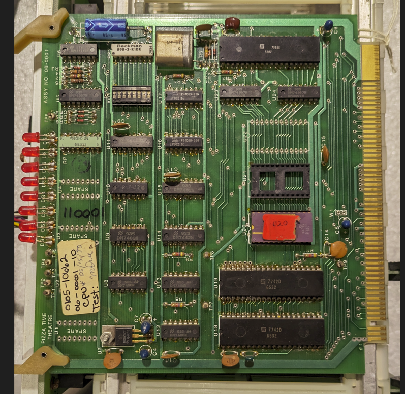
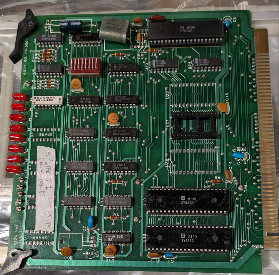
The first board I’m going to talk about is the CPU board for the Chuck-E-Cheese Cyberamic Control Computer. The first generation of this card was designed some time around 1979 according to the schematics and has some design choices that you might recognize. It is made up of a 6502 processor, two 6532 RIOT chips for the RAM, stack, timers, and some I/O, and three 2708 EPROM chips for storing the program. This board fits into a card cage, and only in one specific card slot. This backplane does not have a bunch of parallel wired slots like you might find in an s100 computer of the era, it has a couple large slots for the CPU, Transport, and Audio cards to be installed as well as a bunch of identical slots for character and lights cards to be installed depending on the show configuration.
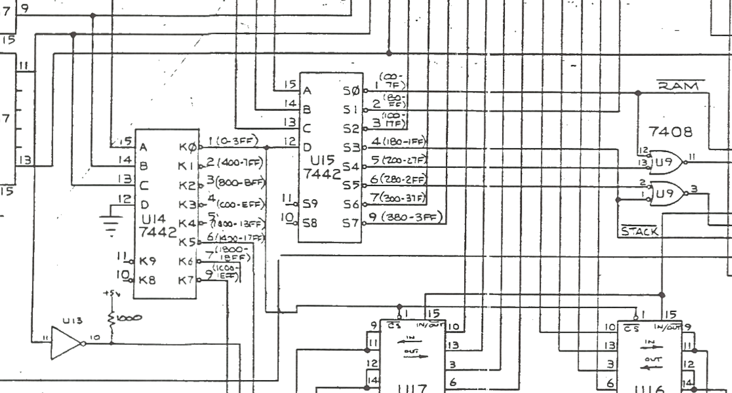
The processor here has an interesting feature in that the address bus was not fully utilized. Lines A13-A15 were not connected anywhere limiting the memory space of the 6502 from 64K down to 8K. If I were designing a backplane I might try to find room for those three extra lines in case I wanted to expand it more later, but for some reason these designers thought that 8K of memory space was enough. The Interrupt line is wired out to the backplane, but on the backplane I have, it’s not connected to anything. Even if one of the other cards was also wired up, this feature couldn’t be used. Those features along with the use of RIOT chips for RAM have me thinking of one thing. This thing is an overgrown Atari 2600. It’s true, Chuck-E-Cheese’s Pizza Time Theater was created as a child friendly place to have Atari arcade games and the design of their in-house animatronics controller shows it.
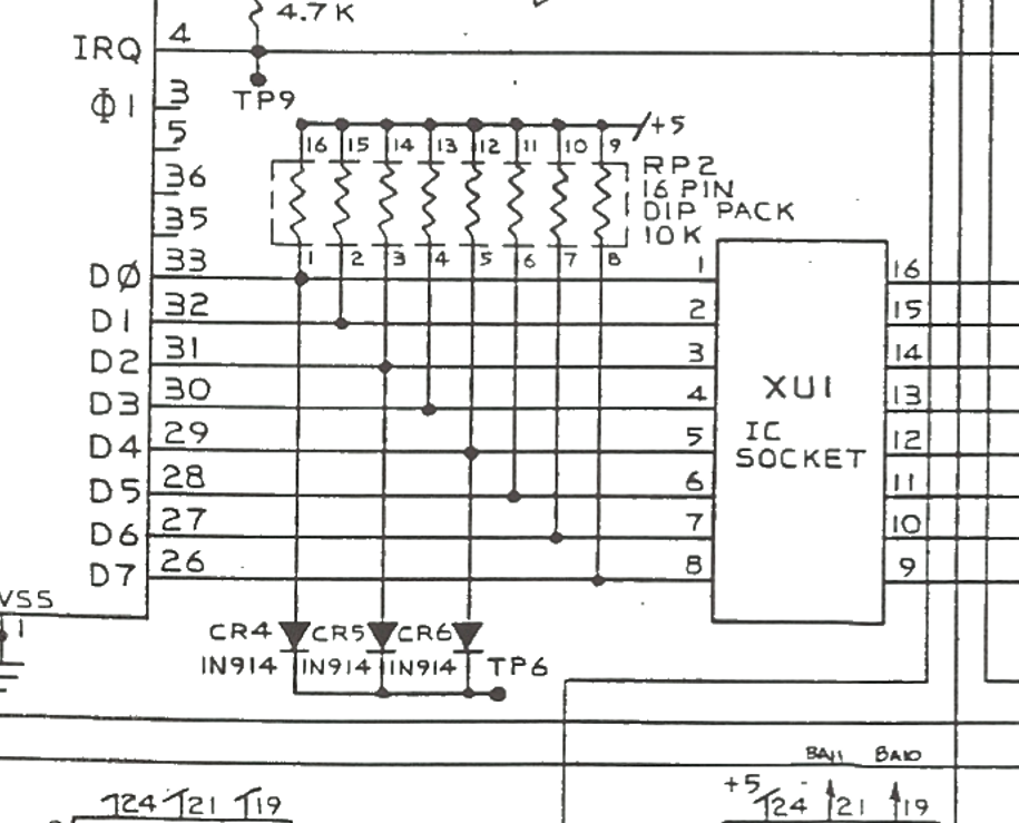
The inputs to this board include a microphone switch, a bunch of buttons that were mounted on the front of the machine (located in a regular 19″ rack), and a rotary switch to set the intensity of the ‘automatic gain control’ for the volume of the show. The outputs are the lights behind the buttons, some lights on the edge of the card that can be used to tell what state it is in, or diagnose problems, and of course driving all the rest of the cards in the system. The address decoding was done by some 7442 chips and each output card only got 8 addresses because they were selected with Address A2-A5. The other sections of memory dedicated to the transport card, the audio card, the I/O, etc.. got 128 addresses per (that’s how much RAM this thing had, but it also had that much stack in the other RIOT chip). The ROMs being 2708s had 1K per and were mapped in at $1400 to $1FFF. How does that work when the 6502 boots from $FFFC and $FFFD? well, not using those last three address lines means that the entire memory map is ‘mirrored’ so that you have multiple copies of the same information logically located all over the memory map. Reading from $FFFC gets the same data as from $1FFC, which is in ROM U20.
There’s also some other cool features of this board. If you want to test that the CPU is working you can remove the jumper at socket XU1 to disconnect the data bus from the CPU and then ground TP6. This makes the CPU execute a NOP instruction continuously thereby allowing you to see if it’s working (the address bus should be constantly counting up). There is a ‘hold’ input to this board allowing other cards in the backplane to effectively ‘pause’ the CPU execution.
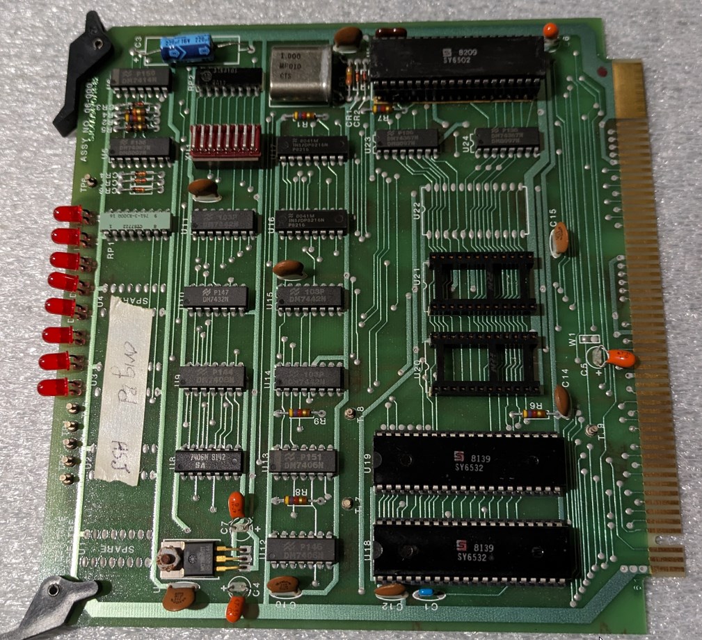
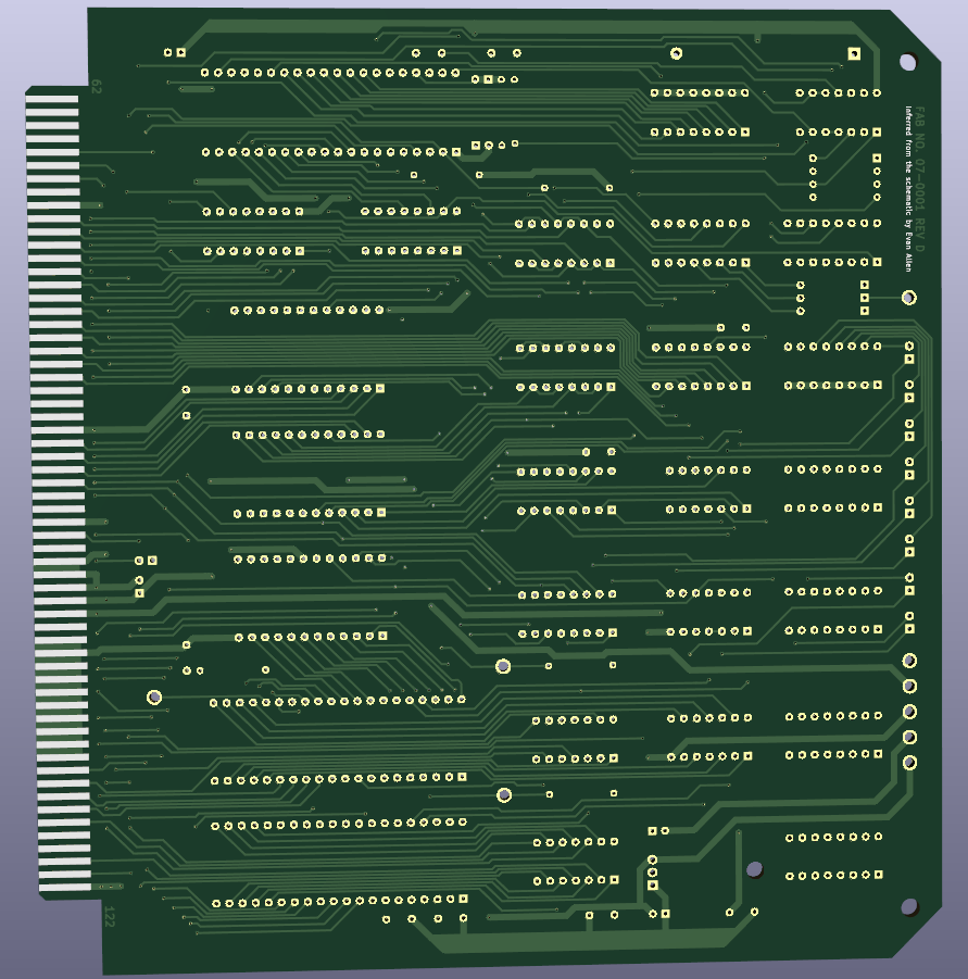
I didn’t have one of these boards to work with, but I had a lot of pictures from three in the San Jose History museum and a couple of schematics to look at. You might think that the schematics are the holy grail, but in the days before CAD, there are frequently mistakes. Heck, in the days of CAD there are still mistakes. Utilizing all three variations of the CPU card that I had pictures of and both sets of schematics I was able to recreate the CPU card 06-0001 revisions A-D.
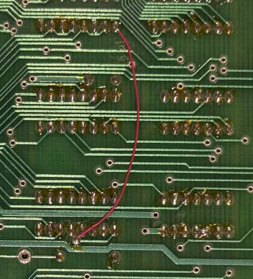
Revision A is the earliest and had several errors on the PCB. Two traces are missing and jumpered to make it work. One trace is made incorrectly and was cut and pulled up. The ground is not fully connected to itself (but since this goes in a backplane that connects it for us). Some pins the schematic claims are grounded are not, that has no effect on performance.
Revision B, according to the paper schematic changelog made one capacitor 16v instead of 10v. This is partially true, but they also fixed the cut and jumpered traces from revision A. They didn’t fix the grounding issues, possibly because they didn’t know about them, and overall this board design seems to be in a good state.
Revision C claims ‘added ref. callouts’ but I don’t know what this could mean as the later schematic has the same reference designators as the earliest one and the board silkscreen is unchanged. The version is incremented in the copper layer text though.
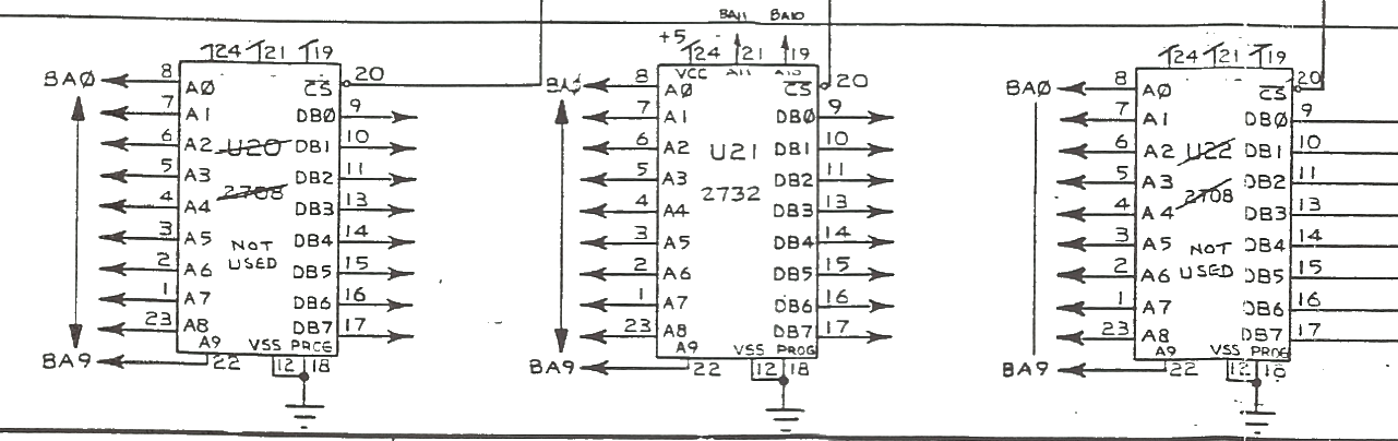
Revision D I have only seen in schematic form and in the way other older revision boards have been modified. This version removes the capability of using 2708 chips and instead substitutes a 2732 chip. The decoding logic is changed to just whenever A12 is high, the 2732 is selected, effectively replacing the 3 2708 chips’ location exactly and adding 1K more memory before each block. The rewiring makes two memory chip sockets useless and reuses the middle one for the 2732. I have seen this mod executed on the revision B board, but never a real one with the traces implemented. To design this one I took a best guess and I think it came out alright. If you’re going to have one of these boards manufactured and you don’t need to remain compatible with a 2708 ROM then I suggest the revision D. I also took the chance to correct the grounding issues because they bugged me (although the real one probably did not).
The 1993 redesign of this system say revision HA, which changed the whole board to use an HC11 processor and also modified the remainder of the data and audio subsystem so it remains compatible only with the old character and light driver cards. I haven’t remade this one because I’m not super interested in rebuilding that era of system, but it’s possible and I have the card to copy.
If you need one of these board I can make you one, or you can find the design up on github here. This goes along with the adapter I made to connect the buttons and lights to the backplane. I will have more details on how the other subsystems work and which versions are compatible with each other coming up. Feel free to ask me about any issues you may have with one of these setups. I may know something after digging so deep into all this.
A while back I showed off this board, but I never got around to testing it. Now I have and it works great. There are a couple things to remember about it though. This board sits on an active phone line and listens for DTMF tones. If you don’t want to use it on an active phone line you will need something like a 9 volt battery or other power source to excite your phone to power it enough to generate the DTMF tones. That’s how the device gets its input, but what about the output? You have a number of pins broken out:
Power Down shuts the chip off when you give it 5v (I recommend grounding it for normal use)
Inhibit stops telephone service tones (A,B,C,D) it gets 5v (usually don’t worry about this, tie it high if you only want to use a regular phone though
Output Enable lets the data bus talk, otherwise it won’t output any data (either pull it to 5v or leave it floating, it’ll pull up internally)
Ready outputs 5v when the data on the output pins is valid, this is important because after a tone is no longer heard the pins stay at the last state they were so this is how to know when there is or is no longer a tone present
Q1-Q4 are the data pins and a binary representation of which tone is being heard will be output on here. You should really use the Ready line to determine when these can be read for accurate tone detection
That’s it. This device does not produce any tones, it just detects them. If you want to use a phone as an input device it’s actually pretty cool. If you want one of these boards feel free to contact me, or if I run out or you want to make or modify the design then they are still on github here.