Archive for May, 2022

TI digital thermostat replacement board

May 20, 2022

Based on the thermostat prototype boards I made, I decided it was time to integrate them. I have this Texas Instruments Digital Thermostat from 1979 that I bought new in box from ebay for like $40. It worked alright for a while but stopped and I couldn’t figure out why. I sent it to Sean Riddle for decapping and he took it apart, optically read the rom, and now it’s in mame! I scanned the PCB so people who want to complete the mame driver can trace the circuitry.

I decided to recreate this as an IoT thermostat, and I had some requirements:

  • Use the original case
  • Use the original display and switches
  • Use and ESP32 WROVER for the additional ram
  • do not use serial or jtag lines for anything else
  • powered from the 24vac from the furnace
  • solid state switching
  • hardware lockout to prevent software glitches running the furnace and AC at the same time
  • temp and humidity sensor
  • humidity control connection

Some of these things I’ve implemented before, some this was the first shot at it. I had done a WROVER dev board before, I had done a max7219 led driver before, but the rest was new. There were some issues, but I’ll start with the solid state switching.

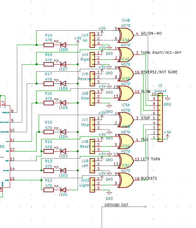
I stole the circuit for the solid state switching from here. He used a different package triac, but mine have worked just fine. This circuit has a fixed design for the 7400 lockout stuff. The fan and humidity circuits have un-needed gates in the circuit, but having at least one buffers the IO from the esp32 and this is replicating the fix I did on the board after my original design fault. I had fan and humidity tied to the ‘enable’ circuit, but that meant you couldn’t run the fan alone. You can see that IO4 enables either heat or cool and IO19 switches between heat and cool. I also had previously used IO16 and 17 which are not usable with the extra ram on the WROVER module, I had to jumper around those. I have LEDs tied to the triac drivers so you can see when the esp is controlling the triac since ther’s no click.

This is the standard LED driver schematic, but I paired it with the pinout for the bubble display on the thermostat.

OK, this one was a complete wild card. I picked a switching regulator basically at random and built the circuit that goes with it. I went to use the recommended parts but the inductor they chose was way too big so I found one of the same inductance but a much smaller size. It probably has less current capacity, worse properties in other ways, but this circuit was a bonus. If it worked, great, if not I’d run 5vdc to the thermostat and call it good. Turns out it was fine.

In order to conserve pins I used a 74hc138 to scan the switches and buttons. This saved exactly 3 pins. I could have saved one more if I made S1 into an additional line like O5 on the ‘138, but using that switch as a totem pole driver for the IO worked out fine. If I gave up on JTAG debugging my design I could have omitted this part. It fit though, and it works fine… now. The part I had forgotten in my original design was those pull up resistors. The input pins I chose on the esp work as inputs but don’t have input pullups so I needed to add those externally… oops. All these problems aside, I was able to patch the board and get it working.

not too bad for a first try

Label everything, silk is free. Add graphics for what connectors mean somewhere they won’t be obscured. Label switches so you can test the board without referring to the case. and don’t bother soldering the un-needed switch contacts. That would just make it harder to remove the switches if you need to salvage them for a new board revision. You can see that I didn’t leave a correct footprint for the capacitor, that’s ok, I just knew I could bend it over and it would fit alright. I also used the screw terminals upside down, there’s enough space for these like this in the thermostat housing and I wanted a quick disconnect for the thermostat.

Also, it totally works! I don’t have code for anything but exercising the inputs and outputs, but it should be trivial to write a simple bit of code to drive it. Writing code to handle the complex programming interface of the buttons is a bit more involved but I want to do that at some point. The project page on github is here, if you have one of these and want a board that can be easily modified to work, I have 4 left. The photo album of before and after modding it is here.

VCP200 breakout board

May 20, 2022

So, I had 3 of these VCP200 chips and I wanted to use them in something so I built a breakout board. In the process I found a bunch of interesting tweaks to the design that I may try in the future, but let’s start with the first one I found and replicated. It’s found in Radio Electronics April 1991.

The whole article has the theory of operation, but the highlight is that the sound is amplified in 3 stages, then clipped, hard, in the last stage to digitize it. This digital signal is fed into the processor to analyze and it picks which set of sounds it most thinks matches what you said. Right away there’s some things I don’t like about this, first is using 4011 gates to drive these LEDs without any series resistors. That’s probably fine, but it’s not my style. Second is that the outputs from this board have series resistors but DON’T got through the 4011 as a buffer. That would limit the current drawn from the chip but not protect it in any way if something pretty bad happened. They also use a 7805 which is pretty standard, but these days we have 5v power everywhere so why would I ever power it from anything but 5v.

After prototyping the circuit on some protoboard (I lost that picture) I made a PCB that I’d be willing to use. This is almost identical for the left half of the board to the design from that magazine. The right half is all me though.

I decided to add LED indicators for all the control lines. I also decided to replace the 4011s with 4070s and using XOR gates as selectable inverters I can configure the signal polarity for any output. If you use this to drive a microcontroller you may not care. If you use this to drive more discrete logic, you may like this built in feature. I had a lot of issues powering this from a usb charger or my bench supply though. What fixed it?

A big cap across the opamp. I think the switching noise of modern supplies just don’t work well for this design. It’s very sensitive. I found that putting it on the back is overkill and I can just add it to the input section, but it’s still worth noting that this circuit works fine on an old linear bench supply, but my switcher was not quite good enough for it.

There was also a layout issue, I forgot the ground pin on the 4070s… oops. Easily fixed though. Now there’s about 5 or 10 variants to the analog part of this circuit that make it more or less sensitive. I think this one works alright. I may do a writeup of the history of this design and the dumping of the rom from this chip later (but we did dump it). I don’t know if anyone still has one of these chips in a drawer somewhere, but I have 3. these boards came in groups of 5. Anyone who wants one can have one (my boards don’t have design fixes, the design on github does).

plusdeck 2c PCI bracket PCB replica

May 20, 2022

I was inspired by this twitter post about using a plusdeck 2c with a MiSTer Multisystem to load cassette games straight from tape into emulators. I wanted to go the extra mile though and use the serial control of those boards. When I ordered my plusdeck 2c from ebay, it didn’t come with the breakout board. That’s surprisingly not a problem though, because the FCC keeps detailed photos of things getting FCC certified.

Well, that’s pretty easy to redo. That has to be most of the traces. Let’s look at the top for the rest.

They made some interesting choices here, let’s go though them. First is the open/short jumper. this is done as a 2×2 header, where I usually see this as a 3×1 jumper, or even as a 2×1 jumper and if you want it open you just hang the jumper off of one leg. This is certainly a choice, just not one I would have made. But what does that actually do? Well, there’s a digital ground and an analog ground. The digital ground is the ground planes by the serial port, that has a plated hole for the PCI bracket screw so it is case grounded. The top screw does not touch the top ground plane because the analog ground is kept isolated. Does this help? well, maybe. The manual just says to connect it/disconnect it to see if sound quality improves. I guess it’s nice to have the option. The next thing is those resistors by the serial port. Enhance!

So… what’s up with this? The bottom shows that pins 2/3/5 are routed how you would expect. Those constitute the ‘3-wire serial’ interface that’s common these days, no hardware handshaking. And for handshaking loopbacks, I’ve never seen anyone use resistors, just jumper them with wire. But let’s go with it’s a loopback, then does that make sense, the way they routed those traces? I’ll skip ahead and say yes, I think it’s what they did. Maybe they were using an SDK that needed hardware handshaking on the serial library, maybe they didn’t know how to turn it off, maybe they’d never made a serial peripheral… I don’t know why they made this wacky decision, but I replicated it how I think it looks under there

that looks sensible, right?

Now let’s look at some of the schematic I drew and the notes I took about the functionality of the connectors. They used TRS jacks that have built in switches so are they doing anything usef ul with them?

The mic makes some sense, they tried to isolate it from the other audio traces by giving it a dedicated ground.

gotta label those pin headers, especially because I am probably not going to populate a shrouded one
label your connectors, color, polarity, function

I used some salvage connectors desoldered from old pentium 2 era motherboards with a heat gun. They used to be in a monolithic gameport/audio connector block but I freed them. I had a heck of a time finding the software and manuals, but I threw them up on the internet archive so no one else has to dig like I did. I have tested the connection and the software does detect the device, but the control isn’t working correctly. I haven’t gone much farther because I got distracted, but I wanted to post this here because I think this PCB design is correct. I plan to sniff the serial protocol in the future to control this device without the bundled software. The ribbon cable is just available on digikey, the rest of the parts are junk drawer finds.

[UPDATE]

I’m an idiot, everything works just fine. The key thing to note here is that the device expects pin 5 of the serial port (digital logic ground) to already be common with the 12v power supply’s ground on the molex connector. If that’s not the case then you have to short the jumper so that digital and analog ground are connected. My test setup was using a bench power supply for 12v and it was not connected to my laptop’s usb to serial converter ground. A note, you need a female to female de9 cable that’s wired straight through (not a null modem) to make this work from a standard PC serial port. I tweaked a bit of the copper fill and made a note on the silk on the bottom about the digital ground situation.

You can use the original software or the reverse engineered python script: https://github.com/natarii/plusdeckctl

I finally ran out pf boards so I posted the project on PCBWay here: https://www.pcbway.com/project/shareproject/Plusdeck_2C_PCI_slot_board_replica_52a2c934.html

I don’t know how much it will cost assembled from them but I reached out to them to make sure assembly will go smoothly. 

Breakout boards, precursor to IoT thermostat

May 20, 2022

I decided it was time to DIY an IoT thermostat, but I wanted to make 100% sure the designs would work first. In that vein I made some generally useful breakout boards to test the design in chunks.

I’ve got a 4x relay board, an esp32 breakout, and a max7219 board for 7-segment LED displays. Each individually is pretty useful, but they make up the majority of open questions I had about making a thermostat. The brains and support passives, the display, and the outputs.

First things first, the relay boards. These were made specifically to use relays stolen from dead or otherwise unusable sonoff basic modules. when those die the relay is one of the only things easy to salvage so I have been keeping them. In addition to that they’re cheap, so I have been using them as a standard relay for my designs going forward.

The schematic is super simple, stolen right from the sonoff basic itself. A single n-fet driving a relay coil in low side drive configuration. A flyback diode (small because i’s a small coil). A series resistor to limit inrush current to the gate of the fet. A pulldown resistor so it is always disabled when nothing is hooked up to the pin. It’s a simple circuit, but I wanted to make sure all my footprints matched my parts I sourced so I just made a little breakout and it works great!

Here’s the SPI 7-segment breakout. I took the standard pin mapping most people use for mapping segments to these SPI LED matrix driver chips. The thing is, these chips are designed to drive a matrix up to 8×8 LEDs, but we’re using each common cathode 7-segment as one slice of that matrix. Since I only needed to try out 6 digits, I left the other part of the matrix accessible as pads. Digits 7 and 8 cathode as well as all the segments to hook them up to are labeled. This one worked perfectly the first time as well, with one small issue.

ESPhome had the LEDs in the other order, so to make it easier to prototype I hacked up one board shown above. I don’t mind having to remap them, but it wasn’t exactly easy with my routing. I don’t agree with ESPhome doing things that way, but whatever, that’s what prototypes are for. I eventually salvaged and scrapped this board for parts, it was very fragile.

the schematic is super simple, and whether I used through hole or surface mount components is usually based on what I have at the time. In this case I didn’t have any 0603 12k resistors, I do now, so my future stuff is made like that. You can also see that I didn’t mark the mounting holes to not show up on the schematic. I also tend to use wire labels without the little termination symbols but that’s not consistent.

Here we are, the esp32 wroom breakout. You can use a module with or without a built in antenna on this one. The issues were that debounce resistor on the reset pin wasn’t hooked up and there’s an extra 10k resistor that should not be populated on a jtag line. I made this to hang off a breadboard and allow some sweet, sweet in-circuit debugging. I based the schematic on the one from the esp-wrover-kit because I was watching Dave’s Garage at the time and wanted something compatible, but cheaper. I compared the schematics of the wrover kit with the esp-prog and took a guess at where to split it and what parts of the schematic were un-needed for me. I got it almost right the first time, but on github those minor issues are fixed.

Always label your connectors, I learned this trick from the esp-prog. I have jumpers on this board to allow it to be powered over the jtag or serial headers, and from either 3.3v or 5v. I think that’s probably a bit much, so for future connectors I standardized to 5v on those headers. That’s not strictly needed, but I think higher voltages going along longer wires is a better idea from a stability point of view. That does mean that the regulator on the target board is needed, but I’m never going to power a board straight from anything less than 5v so this seems fine.

That’s my first 3 boards on the path to an IoT thermostat. You can find them here, I have been trying to keep the repos logically together, but it’s not really working.

Logic analyzer breakout pcb

May 20, 2022

I decided that I wanted an additional logic analyzer, and that means I’m now making a board. I had the design from last time, but it didn’t exactly translate smoothly.

The first issue is the software. I guess the driver installer isn’t archived and sorta fell off the internet? I’m not 100% sure this is required, but I dredged the installed driver off my very old windows 7 install and threw it up on the internet archive. This means the logic analyzer is detected as this device and has 16 inputs, mapped how I laid them out on the board. It’s supposed to make it plug-and-play without setup but the driver being missing and needing to screw with zadig means it’s not exactly that.

Here’s the schematic as it looks NOW but look back at my old article and you will see the pinout for the cypress board I had THEN is different from the one I have now. here’s the board I have now:

new board

Looking at the old one, pin 10 is ground and pin 19 is vcc. This board has them swapped. I don’t need to have them hooked up at all so I omitted them in the current design so the board works with all variants. I also found that they moved some components that moved the relative position of the mounting holes to the pin headers. I designed for the board I had and the new one was different. Cutting some traces before soldering is not hard, you just have to know to do it.

I added a trace specifically that powers both buffers from one spot so it can be cut and you can jumper around to 5v to power the buffers if you want. there isn’t 5v available on the pinheaders or I might have made it switchable. I suppose I still could and I could have a pad where you solder a jumper down regardless, but this seemed like a reasonable solution.

Silk is free, use it. I labeled all the pins, put a pinout for the mapping of cypress ports to pins in sigrok, put the data you need to program into the eeprom, and the device you should get the driver for. That seemed sufficient.

Here is the current design up on github right now, I simplified some of the shapes, moved the hole positions to match the newer board, shrank the PCB to the minimum size, omitted the contested power pins, and kept all the other features. You can either ask me for one of the old designs or go make one of the new ones found here.

Jaguar team tap replica and spinner controller layout

May 19, 2022

I was on a roll making PCB replicas and I hit on one that I haven’t seen before. A from-scratch atari jaguar spinner controller. There’s not much to it, so why not? Why keep hacking up original controllers? We live in the age of 3d printers and super cheap board fab. So I did. The first step was digitizing the schematic to a jaguar controller, so that meant making a replica of my jaguar controller PCBs.

original

These are as close to exact replicas of the PCBs as I felt like doing. The same components will fit, they’re not quite the exact trace layout, but they’re functionally identical. Doing those carbon contacts involved improving a script I found that became a whole different project on its own. That didn’t actually end up getting made either. Like, if you make them they’ll probably work, but I didn’t.

Next I added the wiring to the controller top PCB to make a spinner controller.

This adds the spinner directly to the regular PCB. If you have a controller and want to hack it but the electronics seem beyond you, this can make it into a spinner controller. Now, I didn’t add a switch to this one, so the spinner quadrature is constantly wired to the d-pad buttons. It may not really work because of how 3/4 of the time at least one ‘button’ will be held down depending on where you leave the spinner positioned.

This is the one of these I actually got made. I don’t want to get into DIY carbon contacts right now, but I have a boatload of tact switches with different length plungers. I figured I could 3d print an enclosure that fits this and feels alright. I decided to leave the PCB outline because why not. I also added arbitrary mounting holes because it’s 3d printing and their positions are already in cad, they don’t have to be even. This integrates all the needed circuitry from the bottom PCB into the top. I omitted all the diodes and resistors that don’t matter. This could be the basis for a smaller jaguar controller for games that don’t need the keypad.

It fits!
it works!

For reference, the slider switch is a C&K OS202011MS2QS1 and the rotary encoder is a Bourns PEC11R-4020K-S0024. the rest of the parts are generic footprints.

The last thing I did just because I could. I redrew and laid out the Atari Jaguar Team Tap. No one needs this. There do not need to be more of these in the world. The existing ones can probably be scrapped for parts and it’s a better use of them. But I made one.

The only thing I didn’t replicate (that I now regret) was I didn’t make the ‘154 socket fit both the wide and narrow chips. You can see how the layout would work if those plated holes were there. Does it work? I have no idea. I actually purchased the parts and built one, but I don’t have either of the TWO GAMES that use it. But there you go, you can now start reproducing them. You crazy, crazy people.

You can find all the board files here. I have spare PCBs of the integrated spinner one with tact switches and the team tap if anyone wants them.

XC9572 breakout

May 19, 2022

Frank and I have been working on reverse engineering and fixing/finishing these cheap S100 PCBs I bought off of ebay. These are “DOUBLER” floppy controller and serial controller cards. The first thing I did was scan the blank PCB I got and post it on the internet archive if anyone wants to make a schematic or replica board. This is version 14, as indicated in the copper layer. The only ones I can find documentation for are up to version 2… so what even is this? That will come later, hopefully, but as we read the schematics that are available and trace our PCB we have been putting together what the PROMs on this board should contain. We haven’t done it for the disk controller stuff yet, but we have done it for the serial controller portion. Now, how do we burn PROMs? well, we could try to get original devices and get a programmer for them but that sounds expensive and hard. We decided to go with a CPLD. This one isn’t too old and still supports 5v logic levels. But using this package dead bug is a pain.

wheeeee

That’s not super ideal. And programming it…

That’s some 30ga wire to a protoboard with some pin header on it that we can plug in a knock off usb programmer into. That is not ideal. So what did I do? breakout board!

look at the Rossmann level of flux shine!

I have here a programmer that I modified to supply 5v to the target hooked up to the new breakout and it works great. Let’s look at the design:

Here is the programming header, already wired up to the relevant pins so I can just plug in my programmer. I have pins as breakouts for power, ground, and IO power. I also have a jumper to connect IO power to core power. This chip can run the IO at a lower voltage that the internal logic, or you can run both at 5v. on mine I jumper it for 5v on both, but I left a jumper so these could be more general use boards.

You can see I completely punted on the pinout. I just wanted something easy for me to hand wire. If I need to build this into a project, I’ll spin another design for that, but I prioritized readability of pin names over positioning because I didn’t want to have to resort to the documentation for how I laid out the pins. They’re all there, they’re all labeled, just use it. The files are here for anyone who also needs a solution for older bipolar PROMs. Hopefully there will be follow ups with the setting up of the toolchain in a VM and the fixing of the doubler card.

Z80 PLCC to DIP

May 19, 2022

So, it turns out I had a big pile of Z80 chips, but not in a form factor that I have much use for. PLCC44. All my z80 stuff is pretty vintage and uses the z80 in DIP40 form factor. This seems fine, I’ll just make an adapter PCB. There’s just one small issue. Getting these sockets to play nice is not super easy.

I added an onboard decoupling capacitor because why not

You can see those pins get pretty close together. Let’s look more closely.

Wow. So, those are not supposed to be that close together. It turns out they work, but they are close enough that I wouldn’t stick them there if I didn’t have to. It’s lucky they worked at all, right? well, it may be more than luck. The DIP and PLCC variants of this chip probably use exactly the same die layout. That means that when you put them in a leadframe and wire bond them in, the pins will be in the same relative positions to each other. So it’s reasonable that the pins aren’t completely scrambled, I’m just glad I was able to lay them out and get it working on the first try.

Here it is working in a simple NOP generator to make sure at least that instruction works. I’m pretty happy with this project, now for the cost of a PLCC socket, a PCB, and 40 pins of that nice machine pin header I can have about 20 Z80s. I think I’m actually losing money on that with those machine pins. Oh well. The files are here if you want to use them (maybe tweak it if you have a need to put the tall spot elsewhere)

Simple DIY function generator board

May 18, 2022

In sorting through a bunch of old chips I found a couple XR (exar?) 2206CP function generator chips. I decided to build a small generic circuit around them to make them useful. Even though there are a few different ways to use this chip I settled on a pretty common use with some tweaks for my preferred component form factors and completely ignored the footprints for the potentiometers because it’s my intention to put this board in a small enclosure with switches and knobs for control (panel mount, not board mount).

This is a pretty simple circuit, but I added a couple things because I could.

So, the mechanical decisions were pretty standard. I use M3 holes and round the corners in kicad centered around that hole. I used a standard barrel jack for 12v power in the back, and footprints for components I had on hand. I like using 0603 for passives, either to-92 or sot-23 for transistors, and that little 1117-5 regulator (I prefer these over 7805s these days). You can also see that the jumper positions were placed for layout ease and not for ease of operation because this is for use in an enclosure. I have completely random sizes of electrolytic capacitors so those footprints don’t matter so much, and I really like these hook test points for clipping on to (but why do manufacturers have gator clips and not micro grabbers for scope probes?).

This is the standard square wave output drive circuit I’m using. It’s running through a npn transistor.

This is the circuit I added, I’m using a TTL nand gate as an inverter because I had one. That lets me have a TTL level driver for circuits that would like it. I also used the second one to add an inverted output to it so I now have both signals out of phase from one another, I could envision some uses for that.

it works!

Almost surprisingly it all works the first time. I have two of those function generator chips so I think I’ll build at least one in an enclosure for my own use. I may build up a second one as well to use up an enclosure and one of these chips, maybe not. If you want a pcb, just say so and you can have one of my spares, or maybe one of my spares and the spare chip I have too. If you want to make your own or hack on my design to add a different layout or output stage the designs are up on github here.