This system is more of a concept than a single device, but that just means it’s very extensible. The concept is this: in order to explore, reverse engineer, or repair a system you can run a very small bit of software on the target system’s CPU and interface it to a computer to command it to read and write various IO lines or chunks of memory. How you go about doing this almost doesn’t matter, and we have put together a variety of different ways that may work for various platforms.

The project consists of three parts, the host PC software (interfacing to an arduino’s usb serial port for communication), the arduino as an i2c-to-serial converter, and the target system running a tiny kernel and wired to the arduino. Each of these is optional and can be replaced by other stuff. Let’s examine the simplest implementation: Sega’s Star Trek arcade machine, a Z80. For this implementation we use the demon.py software (either via demoncmd.py or demonapi.py, or your own script) to talk to the arduino, we use the arduino interface software to talk to the arcade board, and we use some already existing input and output pins determined by checking out the MAME driver and schematic for star trek.
; Moniker - Z80 Version
; by Frank Palazzolo
; For Sega Star Trek
;
; SCL  - OUT F9, bit7, (0x80) coin counter 1, pin 5, U11 - R1
; DOUT - OUT F9, bit6, (0x40) coin counter 2, pin 9, U11 - R3
; DIN  - IN  F8, bit3, (0x08) DIP, SW1, pin9, U2-pin 6
;
; Note: We cannot use opcode 0x32 on this platform, or it will trigger
;       the security chip
At the beginning of the z80 assembly code we can see the choices that were made. In the Z80 processor the code starts at 0x0000 so this program will be burned to a rom chip that is placed in the socket of the memory chip already mapped there. The Z80 also has a seperate IO space from memory space, it is accessed with different opcodes but generally behaves like memory reads and writes. We have decided to hook up to two pins of the coin counter for outputs and one pin of a dip switch as an input. It is important that we find 5v logic lines that are (for the outputs) latched to allow for this rather slow implementation of I2C. Speaking of I2C, why are we using three wires? well, getting bidirectional communication on arcade PCBs is a bit difficult, especially since the wires we’re hooking up to were never meant for communication. The 2n7000 FET basically multiplexes the signals together sort of how these level shifter boards do. One thing that’s also noted about this platform is a ‘gotcha’ put in by the manufacturer that means the security chip is triggered by a 0x32.
START:  DI                  ; Disable interrupts - we don't handle them
        LD      A,81h
        LD      HL,0xE000
        LD      (HL),A      ; blank the screen
        JP      INIT        ; go to initialization code
This is also a small amount of application specific code. For this platform we can want to disable the screen before moving on.
; Set the SCL pin high
; D is the global coin counter buffer
; Destroys A
SETSCL:
        LD      A,D
        OR      0x80
        LD      D,A
        OUT     (CCPORT),A
        CALL    I2CDELAY
        RET

; Set the SCL pin low
; D is the global coin counter buffer
; Destroys A
CLRSCL:
        LD      A,D
        AND     0x7F
        LD      D,A
        OUT     (CCPORT),A
        RET
; Set the DOUT pin low
; D is the global coin counter buffer
; Destroys A
SETSDA:
        LD      A,D
        AND     0xBF
        LD      D,A
        OUT     (CCPORT),A
        CALL    I2CDELAY
        RET
; Set the DOUT pin high
; D is the global coin counter buffer
; Destroys A
CLRSDA:
        LD      A,D
        OR      0x40
        LD      D,A
        OUT     (CCPORT),A
        CALL    I2CDELAY
        RET
; Read the DIN pin
; returns bit in carry flag
READSDA:
        IN      A,(DSPORT)  ;0x08
        SRL     A           ;0x04
        SRL     A           ;0x02
        SRL     A           ;0x01
        SRL     A           ;carry flag
        RET
This is the remainder of the application specific code. Because the target system is the I2C master and I2C is a synchronous bus it doesn’t matter how slow or variable the speed commands are sent out, everything just works. That means if it takes another 10 cycles to read a bit than it does to write one then everything is still ok. It doesn’t even matter what the speed of the cpu is on the target system because the arduino is so much faster in this case. The functions above will execute reads and writes to the bits we defined at the top for our hookups. All the electrical necessities for shifting bits, decoding addresses, latching outputs, that’s all already done by the designers of this board, we’re just trusting that they work and using them. But what happens if they don’t work, or if there aren’t easily accessible pins?

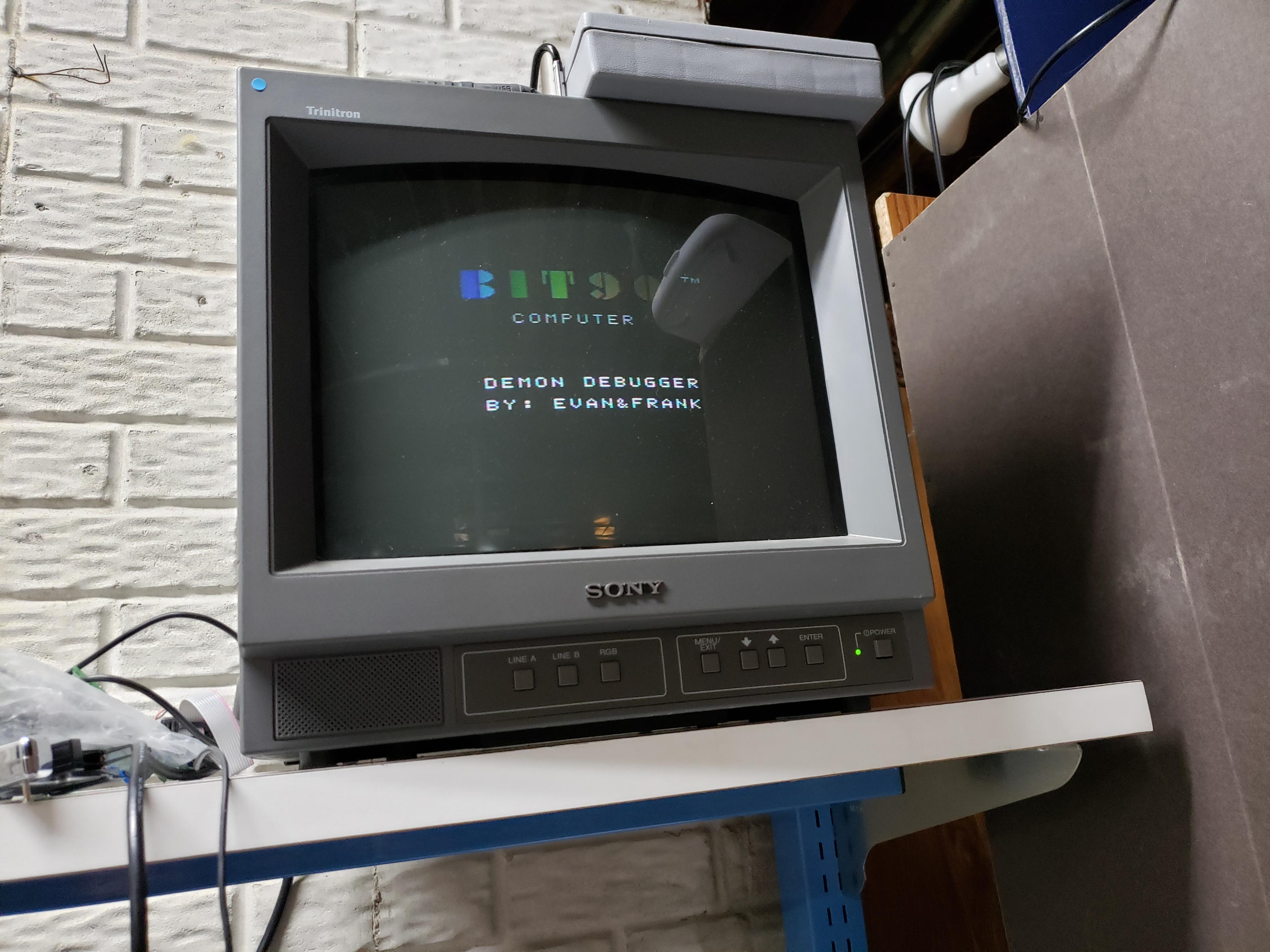
I give you, the Bit90! This is a rare colecovision clone that has built in basic roms and a keyboard. In fixing and reverse engineering it Frank and I developed the next generation of demon debugger: the entirely memory mapped interface. For this we gutted a colecovision cartridge and installed a memory chip containing our code, and two digital logic chips sitting where there used to be more memory.
        .org    0x8000	    ; cartridge start

    	.db	0xaa	    ; cartridge signature
    	.db	0x55

    	.dw     0x0000
    	.dw     0x0000
    	.dw     0x0000
    	.dw     0x0000
    	.dw     START
    	JP      0x0008
    	JP      0x0010
    	JP      0x0018
    	JP      0x0020
    	JP      0x0028
    	JP      0x0030
    	JP      0x0038
    	JP      0x0066

    	.ascii  "BY: EVAN&FRANK/DEMON DEBUGGER/2019"

START:  DI                  ; Disable interrupts - we don't handle them
        JP      INIT        ; go to initialization code
In this code we had some new challenges. The colecovision uses a BIOS, meaning that unlike other cartridge based consoles it runs code off the main board even if there is no cart inserted. This also means we cannot place the code at 0x0000 if we just use the cart slot. The cart is mapped to 0x8000 as you can see above and requires a header to be recognized as valid.

; Set the SCL pin high
; D is the global buffer
; Destroys A
SETSCL:
        LD      A,D
        OR      0x01
        LD      D,A
        PUSH    HL
        LD      H,0xc0
        LD      L,A
        LD      A,(HL)
        POP     HL
        CALL    I2CDELAY
        RET

; Set the SCL pin low
; D is the global buffer
; Destroys A
CLRSCL:
        LD      A,D
        AND     0xfe
        LD      D,A
        PUSH    HL
        LD      H,0xc0
        LD      L,A
        LD      A,(HL)
        POP     HL
        CALL    I2CDELAY
        RET
; Set the DOUT pin low
; D is the global buffer
; Destroys A
SETSDA:
        LD      A,D
        AND     0xfd
        LD      D,A
        PUSH    HL
        LD      H,0xc0
        LD      L,A
        LD      A,(HL)
        POP     HL
        CALL    I2CDELAY
        RET
; Set the DOUT pin high
; D is the global buffer
; Destroys A
CLRSDA:
        LD      A,D
        OR      0x02
        LD      D,A
        PUSH    HL
        LD      H,0xc0
        LD      L,A
        LD      A,(HL)
        POP     HL
        CALL    I2CDELAY
        RET
The act of writing data out is interesting because we are using a rom socket so we can only trigger the chip select line in this socket by reading from the memory region at 0xc000. The output lines we have are the address bus so by reading from various sections of the 0xc000 range we can trigger those address lines to go high or low and latch out a one or a zero to the 74HC74 chip. This act of writing by performing reads is incredibly inefficient without a lot more decoding, but it you have unused rom sockets it is an easy way to get output pins from memory mapped rom sockets.

DATAIN	.equ	0xa000		; where to read data in from
; Read the DIN pin
; returns bit in carry flag
READSDA:
        LD      HL,DATAIN
        LD      A,(HL)      ;perform a read into bit0
        SRL     A           ;carry flag
        RET
Reading is a lot more straightforward. I used a 74ls244 to put 8 TTL input pins on the bus to be read any time you read from the entire 0xa000 range (that’s where this rom chip used to be mapped). For this application I think we use D0 but this method can just five you 8 pins of input if you don’t want to bother with any more address decoding. Some 74xx138 chips could be hooked to the address lines to give you the entire memory space as discrete I/O but that is way overkill for this project, all we need is one bit.
Another success! after learning about how the bank switching inside the Bit90 worked we were able to dump the BIOS and BASIC roms by triggering bank switches and reading from the same section of the Z80 memory map.
The last iteration I’m going to talk about in detail is a setup that fits entirely in a single 2716 socket. The decoding logic is a bit more complex than it needs to be because it’s set up for either a Z80 or a 6502 which need the code to start at different locations, but the setup didn’t end up that complex.

First, this is my somewhat complicated additional demon debugger hardware that is jumper selectable. I had some extra PCB space so I added the 2n7000 that muxes the single direction lines into actual I2c, but in order to keep compatible with existing demon debugger hardware I made it selectable. To the left of the dotted line is the suggested demon debugger hardware on the arduino side. To the right is my new hardware that is incorporated into the target board. The first thing I added was a pull up on the Din (or SDA) line. we had an issue once where the internal pullup failed and we were chasing a bug for quite a while before we found that out. External pull ups are cheap and easy so that could help a setup that uses a vanilla arduino or one with the FET on it. I also added a 2n7000 of my own. In the configuration I show it with two jumpers connecting the outer most pins on that header the rightmost FET is disabled, its gate is tied to ground so it is not having an effect on the Din line and the Dout line is wired to the gate of the FET on the arduino side. If you pull those two jumpers and instead fit a single jumper between the middle two pins you allow the device on the left side of the dotted line to just be a vanilla arduino with no additional hardware. You may also be able to use a buspirate or FTDI chip with no software on it as an I2C slave at that point, but the python code would have to be tweaked to accommodate that. If you were using a demon debugger bit of hardware on the left side you could also connect the top and bottom pins to ground the gate of the FET on the left in case it’s acting up for some reason.

This is the output enable logic for the devil board as we called it. Basically there’s a 2716 or equivalent socket on the target system and we have a 2732 that we use to maps into that space. I used a 2732 so we can have a jumper on the A11 line to get us two programs on one chip. The devil board sniffs four address lines, can inject data on D0, and man-in-the-middles the Output Enable line to redirect some of the memory calls away from the ROM and to our latch circuits. The 74LS74 and 74LS244 are the same as we had in the Coleco cart, but they are now mapped as follows:
; "2716" Memory Map
; X000-X3FF - ROM
; X400-X5FF - I/O (Special region)
; X600-X7FF - ROM
; SCL connected to A0
; DOUT connected to A1
; DIN connected to D0
; "Special Region"
; Read from X4X0 - clear SCL, clear DOUT
; Read from X4X1 -   set SCL, clear DOUT
; Read from X4X2 - clear SCL,   set DOUT
; Read from X4X3 -   set SCL,   set DOUT
; All reads return DIN as bit 0
The input and output all occur in the 0x400 to 0x5FF section of the 2716 as selected by the 74LS139. The ‘139 basically breaks the 0x800 space into chunks of 0x000-0x1FF, 0x200-0x3FF, 0x400-0x5FF, and 0x600-0x7FF. Three of those are routed back to the ROM, but one is stolen and enables our registers when the system thinks it’s accessing ROM. Since we’re setting SCL and Dout at once we have four different sections of memory we can read from, each sets the outputs in a different combination. Every output set also triggers an input on Din because unlike last time the input register is triggered at the same time as the output.
        .org    0x2000	    ; cartridge start

        .byte   0x55	    ; cartridge header
        .word   0x0218	    ; next menu item (first one)
        .word   TITLE	    ; title pointer
        .word   START	    ; start pointer

        ret		    ; rst8
        nop
        nop
        ret		    ; rst16
        nop
        nop

	ret		    ; rst24
	nop
        nop

	ret		    ; rst32
	nop
        nop

	ret		    ; rst40
	nop
        nop

	ret		    ; rst48
	nop
        nop

TITLE:	.ascii	"DEMON DEBUGGER"
	.byte	0x00
In this implementation we installed it in the cartridge of a Bally Astrocade console so we needed a cart header here as well, the astrocade not only has a BIOS like the Colecovision, but built in games (and our demon debugger shows up as a selectable ‘game’. Like the Coleco/Bit90 implementation we set both output bits at once so the functions have to grab what the other bit is supposed to be from RAM and make sure both bits are asserted correctly when the function to assert just one is called.

That’s all the hardware I helped develop, and honestly it’s at a pretty good stage. Some implementations like Gorf or the Astrocade require you to hit a hardware watchdog or the machine will keep resetting, and any new applications will have their own quirks. You can always use something like this PET RAM/ROM board to get some code right into the memory map of any 6502 based machine (still have to locate some I/O or add a version of our devil board to map some in). There’s also a special implementation for the Intellivision based on the LTO Flash cart and its built in USB serial port (so just need the PC side software there). All of the above are various options for the target system interface hardware and some replacements for the intermediate arduino I2C to serial converter. Now it’s time to talk a bit about the PC-side software.

So far I’ve been talking about the platform dependent changes that need to be made, but this is all the common stuff. In addition to those functions to set and read the I/O lines each kernel includes functions that can read and write memory, read and write ports, and start executing code form a given location. That all remains the same for a given architecture (so far the Z80 and 6502). The PC side software is written in python for windows, but should be able to be ported just about anywhere. There is a python API exposed for demon debugger so you can write python code to interface to the target board as well as do some other things. This has so far been used for automating data collection from a rigol scope on the network to improve the Gorf mame emulation colors. This stuff is located in the DEV branch on the github repo so be sure to go there to check out the latest on how to automate the reverse engineering of vintage hardware.
The last thing to mention is that there is an arduino emulator to check out your hardware. using a second arduino uno you can emulate a Z80 target for demon debugger and practice reading and writing memory and I/O before you hook up to a real system and attempt to debug that. If you’ve got a tiny bit of RAM, and a place to install your own code then nearly any system can be hooked up to a PC and the hardware on it can be investigated to see what’s hooked where, or to determine experimentally what is broken on the board.
