Archive for the ‘electronics tools’ Category

Sun Ray 270 to pi/monitor conversion

May 27, 2017

original glory

Sun Microsystems used to be one of the makers of very pretty hardware (if you like the color purple), but that era is no more.  Sun rays in particular are cool though.  The ability to move your desktop with your smart card to any terminal you want is awesome and really, the hardware is really well built.  Also, Oracle sucks.  Combine these two and you have no new hardware or support for a modern ecosystem of sun terminals.  I have tried and failed multiple times to get sun ray servers working and I give up.  I decided to make a decent tiny little thinclient/monitor out of my only LCD sun ray.

custom wiring

The first thought was to just have a pi contained inside it, but it became obvious that I was going to break out other ports from the generic LCD controller.  Doing that and not having HDMI would be annoying, so I added an HDMI switch to the deal.  This did not add much complexity, but it gave me more buttons to put on the front panel.  I decided to use the audio jack holes for the power button to the LCD controller and the input switch button for the hdmi switch, leaving one free to house an RGB LED that could represent which of the three inputs was active.  The power LED for the LCD controller went where the original one did, and the IR receiver went in the corner of the smart card hole.

NEVER trust the silkscreen of the button functions on cheap controllers

It turns out the bulkhead mount HDMI cables I bought have almost the same spacing for screw holes as the VGA ports the sun ray originally had.  I cut and mangled most of the case to fit the new contents and decided to mount as much of it to the LCD as possible so the clamshell could be opened for service.  I also added the 2 composite ports out the original serial port holes as they fit snugly there.

first constraint

The backlight driver went in first, it couldn’t move very far but I put it as far out as I could to leave room for the rest.  Then went the insulating layer (cardboard) and the LCD controller.  With that in and the video cable routed the PI and power supply for it went in easily.  The only hard one was the HDMI switch as it had ports out all four sides and there wasn’t enough space to glue it down anywhere.  After some fiddling it all fit, but I had to add a power switch for the PI because it didn’t like to come up if powered on with the monitor.  This power switch went in the SIM card port that this had for some unknown reason.

all laid out and shimmed with corrugated dead tree

This HDMI switch is actually really cool.  You can only switch between inputs that have signal, and it auto-switches when one comes online.  I’d recommend it for being cheap and useful.

sandwiched between insulating cardboard

This is now 100% more useful to me, it’s a wireless linux box that’s got a built in monitor for working on my single board computers.  I can download and write images right from the second input of the monitor.  If I had decided to spend more time at it I would have lined up the original ports with the USB, ethernet, and other jacks so it looked more stock.  I could have tried harder to get internal sound working on it.  I could have broken out the pi’s gpio to the slot where the smart card went.  This was already a dubiously useful mod for me, and while all those things would have been cool, I really wouldn’t have found them much more useful.

hacked

All of the pictures of this build are here.

TI-58 Calculator battery upgrade

May 15, 2017

After a weekend at Minicon I came back with plenty of goodies thanks to the trusting nature of Amtrak (look for a CDV-715 post coming up) and one of the smallest was this TI Programmable 58 calculator.

original

I love old bubble display calculators, thermostats, stopwatches, whatever I can get my hands on.

crusty

This repair seemed pretty simple, replace the old Ni-Cd batteries with new ones.  The challenging part was someone already did this once before.

you’ve had some cowboys in here…

The batteries were a snug fit, the power tabs snapped, and I ran out of patience.  The original TI charger for this was rated to put out ~3v although after the bridge rectifier easily identified was somewhere around 6V DC-ish.

looks like a rectifier, that can go

I decided that that’s close enough to 5 for 1977 and injected my new power source there.  My selection was based on what I had lying around which turned out to be a micro-usb lithium charger/boost converter that put out 5 volts and a lithium battery out of an old ipod external battery pack from radioshack long ago (I bought it before the advent of common charger/boost converters for single lithium cells).

all kapton’d up

Put together and with some kapton to hold it in place and a dremel to hollow out the case I successfully added usb rechargability to this old calculator.  I will admit that it is now incompatible with some of the add-ons, but I’m not terribly concerned as I intend to use it just as a pocket calculator.  All pictures (including others not in this post) are here.

useful once again

standalone heated bed controller

June 21, 2016

Back in the day when I was at college we had a RapMan 3d printer.  Do not buy this printer.  The version we had was flat-pack, made entirely of acrylic sheets sandwiching smooth rods for construction.  Staying up all night to get the first print got us a small ABS plastic cup and a rain of nuts, washers, and bolts.  If you tighten anything down enough to not shake itself apart you shatter the acrylic, and the controller is proprietary, so there’s not much you can do to it from that front.  We spent the first few weeks designing and printing replacement parts for the printer out of ABS because the acrylic was garbage.  The extruders were nice, but used a custom machined razor sharp worm gear that would just chew up material if it was too soft.  On top of all that, it didn’t have a heated bed.  If you’ve ever 3d printed something you’ll know that a heated bed is quite nice and helpful to get good looking parts.  Since we couldn’t interface with the damn proprietary controller we just built a stand-alone one.

We built this in one night, and to my knowledge it never got changed.  This is both a blessing and a curse.  If you half-ass something and it works ‘well enough’ people are not motivated to make a better one, this could mean even more time before you have a reasonable solution to the problem.  If the solution is truly good enough then it’s not an issue, but there’s a spectrum… The other thing worth noting is if someone decided to take a ‘good enough’ solution out of order and replace it with an un-finished ‘right way’ solution taking the functionality from 60% straight down to 0%.  These sorts of ‘fixes’ are the hardest to come back from because it involves either finishing someone else’s project, starting over, or putting back the first solution.  I would tend to lean toward the latter of these options, but that’s not always possible if the parts have been cannibalized in the course of making the whole system non-functional.

Being built in one night it used what we had lying around, in this case an original msp430 launchpad.  These had a bunch of features, plenty of reasons to like them, and most importantly an arduino abstraction layer ported to them.  Arduino may have a bad IDE with very few features and a convoluted system of adding boards and other support, but the important part is that it’s easy enough to get working fast and has enough of a community that making your first few projects work is super easy.  At the time when I documented projects it was on the IEEE Lab Wiki, considering that’s who it was built for and where people would look for documentation on how to use it.  These days I’m going through my google photos looking for something to document, not to bulk out the number of blog entries I have, but just to put together a repository of my knowledge.  I’m not planning on getting hit by a bus soon, but I bought my own house and am already not that healthy of a person.  Here is the excerpt from the wiki article I wrote:

Overview

The heated bed was purchased to increase the quality of 3d prints on the Rap Man. It is constructed from a bed from RepRapDiscount, borosilicate glass from Lulzbot and our own custom controller built from an MSP430g2553.

Specifications

Maximum Build Dimensions

  • X: 214mm (~8.5″)
  • Y: 200mm (~8″)
  • Max Temperature: 110°C (230°F)
  • Power Requirements: 12V @ 8.5A

Design

We wanted to use one of our launchpad MSP430s, but we wanted to do it fast, so rather than learn how to use TI’s IDE (we tried, there were major problems that varied between chips) we used Energia. Using some KEM-5161BR (common anode) 7-segments driven by 2 74HC595N shift registers. To conserve pins we configured the 8th bit on the second shift register to control the third 7-segment as either blank or display a “1”. We have the POT being read on one pin and the thermistor set up as a voltage divider on another pin. The FET (2 in parallel since we needed more current) hooked up to a digital output. The code is [[1]here].

Future Modifications

  • Replace the thermistor table with a function
  • Replace the on/off functionality with a PID controlled PWM
  • Move the FETs to a separate board (or further away from the pot
  • Replace the FETs with one rated for the current
  • Print a PCB


I’m actually not going to elaborate on that because I don’t remember anything else about the design, construction, or functionality. Looking back, my favorite part of the code is the comment “fitted graphically”, I think I’ll use that at work some time as justification for data.  On the subject of ‘future modifications’ I’m pretty sure none of that ever happened, although at least one person got burned by the FET (that really should have been a relay, way higher power with basically no heat).  This article’s ‘value add’ can be my story and perspective on the whole situation I guess.

pictures are hosted here

code (and an unbuilt board design?) is here

original wiki article for the lab is here

Simple ethernet link tester

June 26, 2013

I have an ethernet cable tester, it takes a 9v battery, has some 4000 series logic and some LEDs and blinks them based on the integrity of the cable.  This new tester takes some nearly useless old technology and makes a fantastically simple device that simply reports the state of the ethernet link to actual running network equipment.  I will state flat out that I got this idea from this instructables article and that I added no content to it whatsoever.  I am posting about it because I want more people to know about how easily this hack can be done, and how useful it is.  To start off with we have an 8p8c to DA15 network adapter.  Yes, I am going to be pedantic about connector naming, see here for the D-subminiature wiki article, and here for the RJ45 vs 8p8c debacle.  This is commonly known as an AAUI (or AUI) to RJ45 adapter, meant for connecting two ethernet connections that are not electrically identical.  The hack is truly simple, just hook up ground and power (supposed to be 12v, we’re running it at 9v) and away we go.  There is also a momentary push button so power is normally off, but that’s optional.

 The two ethernet converters I modified had different indicator lights, the Link light on each light up when a valid device is at the other end, and one even had an Rx light that glows when the network sends broadcast messages.  I have no idea how such little hardware can determine a valid link, but I assume there is a hardware level detection done independent of any actual data transfer over the cables.  The whole gallery is here.

DIY Power Supply

June 15, 2013

This was one of those projects I knew I had all the parts for and it just took being bored one night to decide to actually do it.  I decided I wanted to make my own power supply, not just a modified computer power supply, but entirely from scratch.  This may not have been the best idea since it’s entirely based on linear regulators (I did put heatsinks on them, but no ventilation).  Anyways, here it is:

I should emphasize that I purchased none of the parts to build this project myself, they were all either donated, salvaged, or found.

The base circuit for this I got from here and I modified it slightly to suit my needs.  I decided that I wanted 5, 12, 3.3, and a variable voltage output (at this point I realize I could have done all of this with a computer power supply, but too bad!).  The second place I got inspiration was this EEVblog post, I decided I needed some more equipment and built some.  Now, some design decisions based on parts on hand.

First, it only goes up to about 14vDC.  it was the best transformer I had on hand at the time (although before rectification I read it as about 12vAC, I have no idea why it’s higher once rectified).

Second, I have fine and coarse knobs since I couldn’t find my 10 turn pots (they had ball bearing based planetary gears).

Third, I opted not to have power cut switches for the regulator inputs (space concerns) but I do have output switches. I originally wanted to cut power to the regulators because they would just be dissipating heat otherwise.

<where my schematic would be if I bothered to make one>

OK, now that that is out of the way I can explain a bit of my design process.  I took the base circuit from Raijuu.net and modified it to suit my needs.  I didn’t put in a fuse since I didn’t have one on hand (well, I didn’t have a panel mount holder).  The power connector, rectifier, and power switch are from a computer power supply, the transformer came out of some old piece of equipment, probably a radio, or amp, or something (it was in my ‘transformers drawer’), the large filter capacitor is of unknown salvaged origin.

As you can probably already see the entire thing is put together with computer power supply wiring and ethernet cable (how else would you know I built it?).

Up to this stage we have a 14vdDC power supply with a switch, now let’s get some useful voltages.  The 5v and 12v legs of the power supply were built exactly according to the Raijuu.net schematic, except I calculated the resistor for 25mA (1.2v red LED) and I put a switch between the output and the LED.  The 3.3v leg was basically the same exact circuit as the Raijuu.net variable leg except with r1 and r2 fixed.

The variable portion of this build was the same as the 3.3v leg, I had some pots lying around from an old equalizer whose transformer blew and figured a 1k and 5k in series would constitute decent fine and coarse pots.  I called that a 6k r2 and set r1 toso the max voltage was just below the point where the lm317 started freaking out about not enough input voltage.

That basically covers the entire circuit, the enclosure is a standard radio shack project box I got from a friend’s box of un-finished projects (I think), the screws for this did not come with the box, I assume the originals were pan head and these are not.

The banana jacks came off an old electronic educational board (the sort of thing that exists so you can build circuits with just banana cables).

The project was compressed onto this proto board as much as possible, but the LEDs and resistors were done hanging.


This has been a simple overview of my power supply (I intended on posting this a long long time ago, but I got sidetracked thinking I was going to make a schematic).  

Upgrading the tl866cs, or: misadventures with PICs

June 12, 2013

So, as the story usually goes: I bought the crippled cheaper version and dropped way too much time upgrading it. This time it’s the tl866cs EEPROM programmer. but this thing is much more than that, it does reading and writing of EEPROMs, sure, but it also does avr, pic, 8051, PLDs, all sorts of stuff. The part that sold it for me was that… well, what do you think this programmer is? it’s a micro with IO expanders (or at least buffers), and digitally configurable voltage regulators. so, crap-tons of IO, definable power and ground pins… this thing can test piles of logic chips! all you have to do is apply input signals, take output signals, check against a known good and report faults. So it also tests 7400, 4000, and even ram chips. So this thing is an absolute godsend, it has tons of chips in the database, hex editor built in, configurable pretty much anything.

Now, on to the differences in the versions. I bought the tl866cs variant which has the 40pin zif socket, but no ICSP connector. Don’t get me wrong, it has the cutout, has all needed passives, just needs the header. The full version is the tl866a, what I wanted to upgrade to. Now, as far as I can tell this is an original Chinese design: I don’t know of another programmer in a similar form factor, they have their own GUI (unlike the Saleae I modded the other day). They are understandably hesitant to release any schematics, firmware, or even what chip is driving the entire thing.

Let’s start with the chip. They have scraped the part number off of the package (rotary tool of some kind) and apparently thought this was enough. I won’t even go into the brute force method which starts with the USB Vid is licensed to microchip if I’m not mistaken and they have this wonderful thing these days where you can sort by package to get all possible PICs in that package, then trace power, ground, ICSP, and crystal and you have the family, if not the exact chip (oops, I guess I got into it). The really hard way involves acid and building a complete picture of all it’s specs based on the silicon die, but we’ll save that for military ASICs (You can’t hide from us!). The easy way is to ask around other people who bought it (they are probably electrical engineers/hobbyists, who else buys no-name Chinese stuff like this) and find someone who can read the slightly less worn away chip they got in theirs. Now we have the one unknown part we can proceed to reverse engineer a schematic pretty easily. I know it’s time consuming, but luckily we can outsource that job to people on the internet with more free time than us.

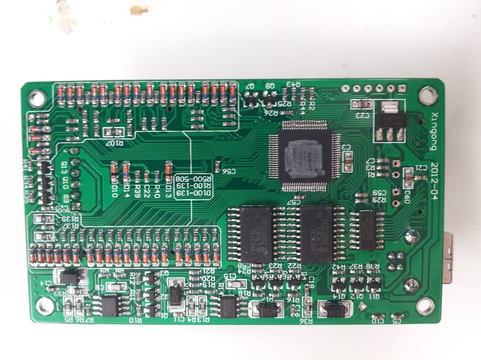
bottom featuring shaved IC and it’s ICSP header… facepalm

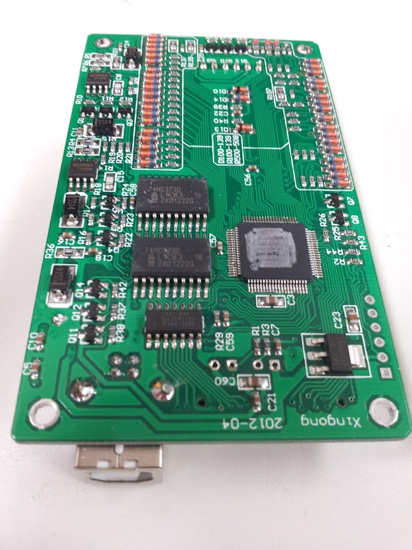
Just a side note on the construction: this board is designed fairly well, I only have a few gripes. It seems fairly obvious that these PCBs are machine assembled and the final product is hand assembled. They use standard 0.1″ pin headers to connect the boards and solder wires to hold them in place. My main gripe is not the wires, they’re redundant grounds, my gripe is those darn LEDs, they are on long leads that go all the way through the boards and solder in the bottom. You’re already putting in all those pin headers, you can’t put in 4 more pins!?

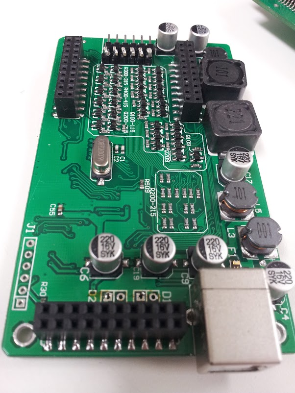
modular pin headers… thank god

Ok, now that we have the hardware, let’s move on to the software. This is where I got hung up, bored, and let someone else do it. We’ll start with my attempt. First thoughts: different USB Pid for each model (so very wrong). we’ll skip my pawing at the minipro files looking for plaintext and move right on to the fact that someone actually discovered that there is a bootloader that takes firmware updates, the firmwares are encrypted, and the bootloader checks them on boot to see if they match. They also decrypted them, reverse engineered the bootloader, created an application to generate bootloader and whole firmware unencrypted hex files with user settable IDs…. duuuuuude, so much work, such nice documentation.

my original serial and dev codes

Now, looking into the future, there is also talk about creating custom chip libraries and chip testing/programming algorithms…. I envision a utopia future where there is a crowdsourced effort adding chips to the library, maybe even designing better hardware (using digital pots to get finer power control than 8 distinct voltages). but I digress…

boost converters on the left

OK, now I have a firmware image to write to the PIC, all I need to do is whip out the pickit3. Oh, I don’t have one. pickit2? Nope, hmm, I have something for PICs around here… AH! here, a microchip mplab ICD 2. Ok, no problem install mplab, and visual studio? I don’t care, whatever, just install it. OK, now how do I set it up? uh, ok, select programmer, blah, blah, error… huh? Well the programmer failed the self test, but nothing’s plugged in to it and it says it passed the test in the settings menu. Uh, we’ll just ignore that. now connect it, import the hex, set the config bits from the hex, aaaaand crap. it can’t recognize the PIC. I don’t know why, the voltages are all fine, it says it’s supported, please work? No, ok, well screw you too mplab. how about some 3rd party pic programming tools. None support this hockey puck of doom. Ok, fine, just use the easy serial programmer. It’s only like five components and I’m in a well stocked lab and…..you want WHAT now?! an 8.2v zener? no I don’t stock those. hmmm, how does this even work… OH GOD, uh, we’ll just forget how they’re doing that voltage regulation… and floating grounds… ok, here’s a more sane one, still needs a 12v zener, that’s ok, I actually have those. Get it all breadboarded up and find out that my 3rd party client supports the PIC18f87j50… with only one of the many compatible programmers he listed. Fine, what else? ok, here, a parallel port programmer, it doesn’t get any more simple. so I need a 74<cough><cough>05, yeah, I’ve got one somewhere, I’m sure it’ll work just fine. Oh, hmmm, it says I need a Vpp of no more than 3.6v, and I think I need logic levels to match. fine, I’ll just lower the voltage on this buffer chip…. crap. it doesn’t go low enough. This is the point where I considered breaking out the textbooks to build level shifters out of BJTs to get the right voltages (I would have already built a pickit2 clone as they can be programmed with the serial thing, if I had the right model PIC for the brain). I just know these chips will work out of spec, what is it Scotty said? “A good engineer is always a wee bit conservative… at least on paper”. Ok, let’s do it. Doesn’t detect programmer… crap. well, it’s breadboarded up, I’ll just… oh… that’s how it checks for this simple programmer, it uses a free input pin to sense the inverse of one of it’s own signals and twiddles it to be sure that, yes, it really is seeing it’s own tail wag. and the pin fell out. Ok, back in, click button, YAY! the programmer is recognized. ok, connect the PIC… one of the pins isn’t used… the one with the bjt… nope, I don’t care anymore, leave it off, keep on trucking. Dump the chip. well, it’s not throwing an error, and it seems to have autodetected the PIC. (yes, hooking up a programmer is exactly all it takes to bypass the ‘scratching off the number’ routine since they LEFT AN ICSP HEADER FOR THE MAIN PROCESSOR OPEN AND PINNED OUT RIGHT). Ok, well, it read something, mostly blank, must be the DRM flag set. Now write the-WARNING CONFIG BITS NOT SET IN THE HEX-. Yeah, they are. No seriously, I open up mplab and import the hex and they’re right there. <sigh> check flag… set flag… check flag… set flag… ok, all are finally set, let’s program. Programming, cool. Errors with verifying, not cool. Well, dump it again, see if it still hasn’t been programmed. No, there’s something different there, quick see if it matches the code I tried to write! huh, slightly different formatting, whatever, where’s the USB cable, plug it in, aaaaaaaand……… SUCCESS!!!!! it is now a TL866A! ok, box it up, now where did I put that AVR ICSP header adapter I made like a month ago…. and it works, no support for the atmega1280 or 2560, but it’ll come, maybe, eventually. this took…. 6 hours, maybe 7? whatever, now I have a decent PIC progammer, never need to do that again.

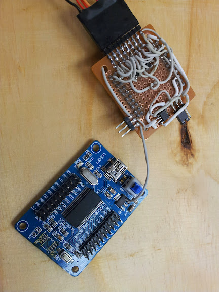
the setup that finally worked

no, it’s not cracked in half, but it does have 5 or 6 pins repaired with solid core wires.

References:

EEVblog thread with all the wonderful info (starts on page 5 or 6)

programmer I used

software I used

rest of the pictures

Saleae Logic clone build

June 11, 2013

So, I wanted a logic analyzer, and I wanted it cheap.  After hearing about the Saleae Logic I was excited, after all what is a logic analyzer but a pile of IO and some nice software.  The thing is, the rate at which you may want to take samples can be much greater than the transfer speed of, say, USB 2.0.  The cool thing about the Saleae Logic, USBEE, Braintechnology USB-LPS, and presumably others is that they use the Cypress FX2 chip.  The main benefit of this chip is that it has an enormous 4 Kilobyte FIFO buffer attached to ports B and D.  That means it can take a huge number of samples really fast.  That chip is really weird, well, it’s the first I’ve heard of having to push firmware to a chip upon plugging it into a computer.  This means that any software that wants to use a peripheral based on this chip can simply push fresh code on boot to the processor, allowing firmware upgrades to be as easy as software upgrades for the client software.  This also means that any software is free to push it’s code to any peripheral and try to use it.  This could be problematic if you end up trying to output into a one-way buffer chip or anything else since the associated hardware could differ wildly from devices utilizing this chip.  The way around this is to have an I2C EEPROM that has the usb Vid:Pid on it, allowing authentication of peripherals to the software.  This method can pragmatically be used for protection, or used for DRM (I think you see where this is going).

overview with crappy cable

There is an open source logic analyzer project known as sigrok that has a client for many different logic analyzers, and a sub-project fx2lafw which is a firmware for FX2 based logic analyzers.  They have a wealth of information about various logic analyzers, especially the FX2 variants.  Some of the stuff I found most interesting was the details on which eeprom and buffer each device uses. Since I am planning on using this chip as a logic analyzer, and as such will be connecting it to foreign/unknown hardware I think an input buffer is pretty important.  I went with the ST DVIULC6-4SC6 because that’s what the Saleae used, it’s fantastically simple, it’s just a diode array used to tie any over voltages to the power rails, so you just tap it right on to your data lines, not through.  The benefit of these is that they’re designed for ESD and can respond even with signals switching at up to 1.65Gb/s.  Now the other thing the sigrok site has for input protection is series resistor values.  Clamping diodes protect from voltage, but series resistors protect from current.  While they don’t actually list the resistor values, they have detailed pictures with which you can actually read the smd markings… except the Saleae uses packages without markings <sigh> whatever, I used 4.7k 603 package ones between 2 pads on a standard perf board.

close up of my hackery

My original plan was to break out all 16 pins of the FIFO (prots B and D) so that I could have a 16 channel logic analyzer, but ST only samples one of each part and only had 2 variants of the ESD chip, so… I’ll do that later if I really want it.  Now I just needed to figure out the EEPROM problem.  I bought the Lcsoft CY7C68013A Mini Board off of ebay for ~$15 it comes with an EEPROM on it and a jumper to set the address of the chip, the problem is the chinese company used an EEPROM with 16bit memory addressing and put it at the address where the Saleae looks for an EEPROM, except the FX2 needs an EEPROM with 8bit addressing at that address, and the Saleae won’t look at the address where the FX2 will allow a 16bit addressed EEPROM.  Basically, while they tried to create a knock off, they failed.  I know they tried to create a knock off because I dumped the 24c128 they had on the board, it had the right USB Vid:Pid on it for the Saleae.  Well, it’s fantastically easy to find EEPROMs of the required interface as they are used all the time as the DDC chip in any VESA compatible display (VGA, DVI, or HDMI ports each have one) to communicate to the computer what resolutions a monitor is capable of.  There is a way to use the Cypress tools to reprogram the EEPROM if you don’t have any other tools to do it, but I just used my tl866cs, fantastic programmer (trying to upgrade it to a tl866a).  I salvaged a few from the logic board of a long dead and smashed LCD, wrote them with the required bytes and voila! we have a Saleae Logic.  but that’s not enough, oh no, I need to make this better than retail.  How about making it also a USBEE ZX? well, kinda.  I have yet to figure out what pins on the FX2 map to the Trigger and Clock on the USBEE ZX.  Also, I have some sources that say the USBEE ZX is not as picky about the EEPROM type as the Saleae is.  And I needed to solder a jumper from the board to the protoboard since 5v isn’t broken out on the headers (for the GND, 3.3v, 5v header).  So, I grabbed another EEPROM, burned in some new Vid:Pid bytes and hey! it works too!

yeah, I soldered a wire, boo hoo

Fabrication took place in my signature style: using whatever I had lying around and not bothering to etch a board.  Don’t get me wrong, I can etch a board in a few hours with the tools at hand, I just didn’t feel like it.  “But they’re surface mount chips” I hear you cry.  “But I don’t care” I respond.  Some people invest in rework stations and reflow ovens, all I need is a really, really fine tip on my iron.  Not for this project though, a regular fat tip will do just fine.  “How can you solder those chips down? the pin pitch isn’t right”.  Ok, fine, scrape off 2 circles of copper and straddle it with the EEPROMs tack the corners and the 2 center pins on each side aren’t soldered to the board.  “But you have 2 EEPROMs…”.  Do I even have to say this one? Stack them, wire all pins in parallel except the SDA line, switch that one with the jumper.  “Ok, fine, but the SOT23-6 don’t stradle like that, ha!” Ok, fine, shave off half a pad, straddle the middle pin over that space.  “Hey, you should get some 30 gauge kynar wire for that, works great”.  I’d love some… oh, you’re not offering? well then, scrap 40pin IDE cable it is.  Some fantastically cheap 0.1″ female headers from ebay (not breakaway, but at these prices I can sacrifice a pin every time I want to shorten them), scrap male headers from an old motherboard, and a jumper from a dead IDE CD drive, and a bit of nearly new protoboard, now I’ve got a logic analyzer.

Features:

8 channel logic analyzer + ground pin

jumper to select which EEPROM

in line resistor protection

diode clamp protection

GND, 3.3v, 5v header (on the USBEE)

power button

Things I missed/messed up:

USBEE trigger and clock pins

ground pin should be on other side (to match Saleae)?

PORT D (remaining 8 pins for use with sigrok)

References:

’C0-A9-08-05-00-84-23-00′. this is the VID:08A9 and PID:0005 for the USBee ZX device. ‘C0-25-09-81-38-1B-00-00’. This is the VID:0925 and PID:3881 for the Saleae device.

PORT B[0:7] => Saleae[purple:black] (I think that’s the correct order)

Links:

list of FX2 devices in sigrok

my board

what I’m trying to emulate

the other one I’m trying to emulate

original inspiration (gave me the EEPROM info in the comments)

gave me the Vid:Pid

lots of useful info, just not essential to my project

how to write the EEPROM if you don’t have any other way