Archive for the ‘projects’ Category

Ipod fm transmitter mod

March 22, 2014

Final product

I had an Ipod FM transmitter, tonight, and I wanted an android one.  I fixed it.  This is my method and the specifics for this model.  The main reason I couldn’t just buy one is because I have an otterbox defender on my phone which is great for protection but eliminate most docks.

The original state

This dock is the Belkin TuneBase FM model F87176 (mostly there to get indexed by search engines because when I searched for a hack for it I didn’t find anything).  Opening it up I find a whole pile of test points very well labeled, interesting things like RX_IRQ, C2CLK, C2D, LCD_D0, a bunch of voltages and a bunch of others (pics in the album).  I didn’t touch any of them.  I’m sure there’s something cool there, maybe the interface between the 8051 (not kidding) and the fm transmitter, maybe the screen’s display (almost certainly), maybe even something more interesting.  I can’t imagine what I would add to this with that data, so I just filed it away for later.  The first thing I did was pin out the ipod connector:

really bad picture

Luckily the connector was less blurry in person and pith the help of pinouts.ru I worked out what all the pins did.  One of the things I noticed was that I couldn’t change the station when the ipod wasn’t plugged in which told me that the ipod was probably connecting a pin to ground (connecting the ground pins together is what it looks like from an analytical point of view) and I determined what one it was.  When I shorted those pins together I could trick the dock into letting me control it without an ipod attached.  The grounds get all connected, the 5 volt output that went to the ipod now goes to the android phone and the analog audio inputs go there too.  The challenge now is to make the android phone output audio on it’s usb connector.

pinout

The phone I have now is the Samsung Galaxy S4 (t-mobile)and it’s similar but not identical to the S3 and previous galaxy phones.  I found it here that the samsung phones set the mode with a resistor on the id pin (some of them do a massively more complex scheme, which is awesome but not relevant here).  The pin numbering is laid out here for left and right audio (It turns out that this dock outputs something on the order of two amps which is great for navigation).  The S4 specific data is… somewhere, but the main point was that car mode and desk mode got combined.  The final pinout had a 365k ohm resistor between ID and GND, I used a 5% 360k and it worked fine.

The test setup piped audio to my speakers and worked perfectly.  After that I soldered up the car dock to the adapter (power and all) and tested it in my car.  I can’t overpower the obnoxious station near me, but on empty bands it works ok.  It’s a bit more quiet than I would like but whatever.  After I cut the ipod connector off I widened the connector hole for the usb micro connector and glued it in place with the phone plugged it.  Once it wouldn’t move much I finished potting the connector.  Now I had a car adapter, but since usb micro connectors are the shittiest connector on the planet full stop I decided to bend a bit of sheet metal into a holder to prevent side stresses when I drive around corners.  Glued that on and now it’s done.  Very simple hack, but some people don’t have the experience to know how easy it is.  The documentation is a bit sparse, but I’ve got some keywords and sources so I think this can probably be accomplished by anyone.

IBM model M…122key?

March 17, 2014

I was at an electronics thrift store recently (I’m not advertising here partially because I don’t care that much, partially because there’s another one still there and I may go back for it).  to get something, but while I was wandering around this caught my eye.  I originally called it an “IBM Model F” but that’s wrong, it’s a Model M, but it has 122 keys.  It does self identify as a “Plt No F3” but that may be a coincidence.  What I can tell you is that it’s a part number 1390876, was made in 1987, and someone warrantied it until 1998 (maybe?).

How’s that saying go? “This is my keyboard, there are many like it, but this one is mine”.  Well, in this case there are none like it… anymore.  I decided that there were some aspects of a bunch of different keyboards I wanted to incorporate into the layout of this one.  I started by deciding what I wanted in my keyboard.  First I wanted to make sure all the keys had a useful function.  Second I wanted to use as many keycaps from the original layout as possible.  Third I wanted to have numlock on at all times (or rather never have the keypad do anything but numbers and math symbols).  Next I needed to put back a windows key on a keyboard distinctly lacking one.  The arrow keys had to be restored to a sane configuration.  Finally I wanted to have commonly used key combinations assigned to single keys.

The keyboard as it originally looked

I really liked some of the historical things this keyboard brought to my attention.  There are a bunch of symbols that are present on it that I’ve never seen before.  The number one has a shift function of a pipe rather than an exclamation point.  The problem is that the pipe key looks the same as it does on more modern keyboards.  That’s actually a broken pipe symbol which used to be a different character (but for some reason the broken pipe symbol remained on the keyboard while the use moved to the pipe).  The alternate function of the six key was a bar with a hook on the end which I have been told used to represent a logical “not” state.  I’m pretty sure I can’t pass that as a HID keycode and have any modern operating system handle it.  The exclamation point is occupying a key with the “cent” symbol, which falls into that category of ‘symbols we don’t really use in modern computing’.  I liked how the numpad didn’t have numlock functions defined on it, but unfortunately the plus sign is occupying the spot the enter key does (and I use that one a lot).  I do have another key to play with however as there are two normal sized keys above it rather than the large key that’s usually there (and I put the small return key on one of them, and a carrot on the other).  The number of keys that IBM didn’t even bother to define I found interesting.  The function keys are plentiful, but I wanted them to be ‘f’ keys, so I switched those.  The pointed brackets (or greater-than/less-than symbols to some of you) were on the same key, I thought that was interesting, but I decided to mostly put it back to qwerty in the major ways.  I kept the funky enter key (‘field exit’ it says) and that moved the pipe key down.  The left shift key is smaller on this keyboard, I chose to put the windows key there.  The arrow keys got moved to it’s proper configuration and I put a context menu key below it (what else would I do there?  The left ‘alternate f keys’ I decided to take direction from the sun keyboards and map things like copy, cut, and paste there.  I also added some others I found useful in web browsing (the ‘untab’ key as I call it was present on the keyboard, but in the cluster above the arrow keys) and one that my Lenovo T60 taught me about (next web page).  The top row of the f-keys I went with media keys, a print key that was on the keyboard originally, the scroll lock cluster (which isn’t on this keyboard anyway, and I didn’t need scroll lock) and the escape key.

Sorry about that, there’s no real logical place to break that block of text up that wouldn’t just be arbitrary.  I liked that some of the keys had symbols and no text as opposed to modern ones (backspace, tab, caps lock, shift, untab, return) and some had less than entire words (del, ins).  The controller is the brainchild of a fantastic guy on the geekhack forum by the handle of Soarer.  I found out by reading the entire forum thread here that the code (or maybe documentation) wasn’t released for so long that someone else developed an alternative that now has other and different compatibilities (which is kinda cool).

The hardware is trivial, it’s just a Teensy 2.0, a keyboard connector and nothing else.  The teensy is really great for being stupidly cheap and able to act as a USB HID device.  The teensy 3.0/3.1 is out, but that’s a full 32bit arm processor and so many levels of overkill that I couldn’t bring myself to consider it for this project.  I chose to add the three indicator LEDs because this keyboard doesn’t have them.  I also chose to add the reset button in case I wanted to put on a new teensy firmware and didn’t want to open the case.  The last feature I added was that I broke out all the aux inputs as 1/8″ headphone jacks.  I did it wrong.  I shorted the ring and tip together and connected them to the aux input and the shell to ground.  I should have connected the shell to ground and the tip to signal.  I now have to use stereo male phono connectors because mono ones short it out and have the key constantly pressed.  I really like the aux inputs for things like footswitches, I mapped them to left and right, (for surfing image galleries) space for a pause key, (watch this space for a laser line break switch using a comparator) and page up and down for surfing blogs.  The footswitches I had were normally open and normally closed.  Opening it up, bending the leaf switches apart, and flipping the switch over was all it took to make it normally open and work with the controller.

In the end I decided to label the keys with my dymo letratag (free after rebate from black friday a long time ago) and I have transparent keycaps on order to make them all the same height (and protect the labels).  I’m also looking into having key caps printed up, but it may not be possible (the company says they do it but some people say they’re unresponsive).  The firmware for the keyboard is seperate from the re-mapping and macros.  The config file is compiled into a binary form and uploaded to the microcontroller.  The code allows for all sorts of cool features and the documentation tells all about it, but I’ll mention a few things here.  You can make macros without using any modifier keys (alt, ctrl, shift).  You may also want to use a more conventional ‘MAKE’ ‘BREAK’ keypresses rather than the ‘PUSH’ ‘POP’ that are supposed to restore the keypresses to the original state.  I had problems using my ‘shift-tab’ key with the ctrl key to make ctrl-shift-tab so I chucked all of the ones I wanted to use in combination (and my config file reflects that).  I also had a problem with the PAD_ASTERISK keywhere I remapped things in the wrong order, causing two keys to be the ‘carrot’ key (the fix was to make the PAD_ASTERISK a macro from it’s original key rather than a remap.  I think that’s all the oddities I found, but I didn’t even try to use the layers function or some of the other stuff.

The world’s most obnoxious keyboard now has USB!

Continuing adventures!

Microwave oven repair

March 16, 2014

So, another round of posts to relieve the backlog of ones that I have pictures for.  We had a wonderful microwave at the house I lived at while in college.  It had all the features I could ask for: a temperature probe.  I know some people want power levels, digital interface, or even a rotating tray, but I really really liked the idea of a temperature probe.  I wonder why modern microwaves dropped this fantastic feature.  My instinct says that morons think “I’m not supposed to put metal in the microwave, therefore I can’t use this feature supplied by the manufacturer”.  The ability to put metal in the microwave has been proved as a fantastic way to heat a solder pot or melt pewter for molds (and it is not bad for the microwave).

Now, I mentioned this microwave didn’t have a rotating tray.  That’s not true, it came with an aftermarket one, but no rotation mechanism.  My theory is that the mechanism had an electric motor on it and it turned quite well until someone lost it before we bought it.  I also mentioned it didn’t have a power level selector.  That’s also not true, it had one, past tense.  This time it had one when we bought it and it doesn’t now.  I’m the one who removed it and I don’t feel bad about it.  Originally the switch was sparking and eventually died as seen here:

The fix I originally had for this was a set of switches that replaced this one (I’m NOT trying to source an equivalent to that).  That worked for a while, but eventually we had a problem of complete failure of the power system.  That is shown here:

The method this microwave uses to change power levels is literally by dissipating it through a huge power resistor and switching parts of it in and out of the circuit.  This method is less efficient than modern methods of sending pulses of full power followed by no power to the magnetron, but much more regular and produces a smoother pattern of heating in the microwave.  A nice big 120W wirewound resistor would be the best idea for setting power level, but that’s prohibitively expensive and I’m just too lazy to look.  This microwave got shorted to full power for the remainder of the time it was under my care.  I’m not sure what happened to it, but I’ve only seen one better than it and that one had digital controls, a temperature probe and a rack!

Inside this microwave I found schematics and testing procedures, as it turns out our magnetron is operating within normal parameters of full power.

Schematic

Manual

Wake-On-Lan Powerstrip

January 20, 2014

For the one of you that has this blog as an RSS feed you’ll probably have figured out I’m not staggering posts, I put the information out there just as fast as I write it.  I’m not looking to build a community, but more to be indexed on google so that people who are looking for help on specific subjects can get it.

This is a project that is a blatant rip-off… I mean derivative of a hack made by a friend of mine over at the i3Detroit hackerspace. His hack used the Wake On Lan feature to reset a server, mine could be used in the same way, but I tend to use it as a fancy lightswitch.  That article I linked to has a fantastic description of component choice that I won’t try to duplicate here, I’ll just go over the implementation I used and how it differs from his.

I will first start by saying that this design has gremlins.  It took me way longer to transpose the circuit from paper to breadboard and have it work, and I gave up trying to convert from breadboard to protoboard around attempt five or six and just started soldering components together and rolling up the breadboard circuit into a solder blob (which functions to this day).  I have since designed a board for this project.  I plan to eventually roll it into a tindie (or kickstarter kit campaign) but until I get around to that you can do it yourself with the provided schematic and eagle board files.  Feel free to make a surface mount one as well if you feel that adds much benefit (it’s just a cost savings in board fab and parts, the size is already as small as needed (as small as the network card is).

design document

My modification to the circuit uses the output pulse from the 555 timer to trigger the clock input of a D-latch (wired as a flip-flop) through a FET.  Let that sink in for a minute, read it over a couple of times slowly.  The last bit uses another FET to drive a relay based on the output of the flip-flop (a relay attached to the power strip).

breadboarded circuit

OK, so let’s start with the “through a FET” part.  A Field-Effect Transistor is a transistor that has an amplification curve such that it is effectively an on/off switch.  That means that while it is truly analog, if we use it right it can very easily be used to just pass whatever current you need with a small signal.  In this case I’m using it as a buffer so the 555 timer chip doesn’t have to drive the flip-flop directly.  This is overkill, but with the amount of trouble I had making this work in the first place I though it wise.

Now we’ll tackle the “D-latch wired as a flip-flop” part.  So, this may be a well known configuration (and having a bachelor’s degree in EE now I should know that) but I came up with it independently of anyone else.  The latch takes whatever is on the input and puts it on the output when the clock pin is twiddled (rising or falling edge, I’m not sure).  The chip I chose has a complementary output, that means they have the opposite of the output on another pin, so when the output is at 5 volts, the complement is at 0 volts and vice-versa.  I used this to my advantage.  I wired the complement to the input so that whenever I clocked the chip the output would change to the opposite as I latched in the complement to the output.

The modification I suggest is that rather than oscillating the output you could have two network cards with two MAC addresses and when you WOL one it turns on the relay, and the other turns it off, regardless of the state beforehand.

blobs that work so well

After this picture was taken I decided that having the neon lamp indicate status would be preferable because the one on the powerstrip sucked.  The blob on the left is the 555 timer, the one in the middle is the latch, and the one on the right is the relay.  The whole thing is built into a computer power supply body and powered off of a salvaged 5 volt wall-wart.  The software I use is either wakeonlan for linux or any wake on lan client for android and I can blip the power from the internal network.  If I can ssh into a server on the network from the outside then I can blip the powerstrip from anywhere on the internet.  That is not really useful because there is a small chance of the circuit bouncing (an RC damper could help) and my current one doesn’t turn it off, it only changes the state.

whole thing

There it is, a way to use up all those PCI network cards wasting space on your shelf.  No code, COTS parts, and you can flip a bit on your network.  This is essentially a network attached bit, get 16 (one for on and one for off) cards and you can have a very very slow 8-bit bus.  Throw on two more for a strobe line and you could bit-bang a dot matrix printer on the network.  The cool thing is that you can literally solder the input 8p8c (RJ45 to some of you) jacks in parallel since they’re passively receiving.

The eagle layouts will go up just as soon as I go home and upload them.

EDIT:

Eagle layouts are up now, I invite you to do better (because it only took me a night).

design for though hole component version

LCD monitor repair (again)

January 19, 2014

OK, so this is one of those days that starts with big plans and gets derailed seemingly because those plans were so well thought out.  I come from a group of people that spend their days just repairing things because they’re there.  We have taken it in stride to develop techniques for repairing commonly thrown out items and apply our experience to new items as we get a hold of them, but we rarely document our work or share our knowledge beyond the confines of our lab.  This is the story of what happened when I tried to document what I figured would be a routine repair on a common model LCD monitor.

I never know what to put in this text

Our Patient

The monitor (as you can see) is a Dell 1907FPt 19″ widescreen LCD monitor.  The first thing I recommend when you have a device of any kind to repair is to look up that model (or series) and see if anyone else has encountered problems with it.  Hopefully you’ll run across a helpful blog post of someone who took the time to explain the steps they took to debug and fix theirs, so you can cut down on the time it takes to fix yours.  I, of course, didn’t do that.  I have no idea what the common failure modes of this monitor are and what the commonly accepted fixes are, so I blazed my own trail to some hilarious consequences.  Seriously, do as I say, not as I do.  For every blog entry of a moderately successful hack/repair I have there are a dozen failed ones that could usually be avoided by spending some more time researching and less time breaking things.  In the future I hope to post my failures with notes for future pioneers, but my successes are usually still around after the fact so photos are easier to take (since I almost never take them during the event, but months after).

Now, having opened more than my fair share of Dell monitors I thought I’d itemize just what steps are involved.  First you need to remove any visible screws, this usually just consists of the four phillips head bolts on the back (seen above).  Next you need to insert a spudger (yes that’s a technical term, look it up) into the gap between the monitor back and the bezel.  That separation into two pieces is the entirety of the plastic casing on this model.

seriously, adding content in secret? I already have a title and caption, what else can I possibly add to this image in this way?

step one

tabs exposed

keep going, almost there

and there you go, dis-assembled

Once you get the back off of this monitor you will inevitably hear a clatter as something falls to the floor and hides among the junk there until you figure out what exactly was missing so you know what to look for.  What you are looking for is a small plastic button and spring that retains the base to the monitor.  The button is a Dell thing, they have brackets on their stands that allow you to use your monitor with only that stand and not that of another Dell monitor.  These stands are “tool-less” which is slang for “our main consumer base can’t operate a screwdriver”.  The monitor itself has VESA standard mounting holes, but the stands are mostly useful for the monitors with which they came (although I may explore the hacking I have done on these stands in a later post).

The button and spring, free without the back

carefully remove this ribbon cable and the double-stick tape that holds it to the monitor casing

Now we need to just keep removing screws and remember where they came from.  You can usually ditch the shielding if you don’t care about potentially harmful interference as covered in FCC part 15.

remove one cover over the inverter wires

and the other

remove the inverter wires from one side

and the other, while you’re at it remove the screws that hold the monitor to the controller board housing on both sides

the panel without any controller, power supply, or inverter

now remove the screws that hold the heatsink to the casing

screws seen here (note they are flat, they mount flush with the panel

power supply board has had it’s screws removed

mains plug with screws removed

screws in question

Not pictured (I know, with all these pictures I forgot one) is the removal of the logic board’s retaining screws and the mounting hardware for the d-sub connectors (VGA and DVI, although DVI’s not a true d-sub).

controller board

Here is the controller board.  There were no bad caps on it, which is a shame since that would have been an easy fix (unless the problem caused a chip failure).  On the bottom are the ports exposed to the outside.  DVI, VGA, USB-b, and a dual stack USB-a.  This particular monitor has a four port usb hub built in (which I’ll go into later).  The port on the right side of the board is for a two-usb port daughter board for the hub (only passives if anything).  The ribbon port on the right is for the front panel controls (bonus points to those of you who remembered that ribbon from earlier).  It is noteworthy that different versions of Dell UltraSharp monitors use different pinouts for the cable with different numbers of features, but they all seem to use the same size cable and connector so they are interchangeable as far as that goes (buttons have different functions, or no function at all).  The port on the left is for power input (it could be pinned out, but I didn’t as they’re usually labeled).  The top port is the LVDS signals to the LCD panel.

close up on VGA and DVI port electronics.

So, the three chips here are two i2c EEPROMs and one chip that I assume is the receiver for the VGA signal.  The eight SOT-23 packaged devices to the left are probably FETs being driven by the differential signalling on the DVI port (the same as the monolithic analog receiver for the VGA port.  The EEPROMs are of note because they hold the EDID information for each port, they tell the computer that’s connected to the monitor what resolutions are supported.  The noteworthy fact is that these type of EEPROMs are massively useful as they’re easy to reprogram and use in things like PCI network cards, motherboard BIOS chips, and USB peripherals.  The chip with the little white sticker on it is probabbly the i2c EEPROM that holds the settings for the Genesis main controller, setting what the settings on the LVDS panel are.

This is interesting to me because you can now buy generic LVDS driver boards and inverters to make use of that surplus laptop LCD panel and I have this thought that I could re-purpose one of these drivers to be used on a different panel.  This phenomenon changes the standard answer to the question of “I can hook the composite signal of my n64 to this old laptop panel” from “No.” to “Maybe.”.

USB hub

So, this circuit is interesting, it’s a USB hub.  The USB hub is entirely separate from the controller that drives the LCD except for power.  I have in the past had good results tracing out the power for the circuit seen here and cutting power to the rest of the board to use it as a stand-alone hub.  The thing about powered and un-powered hubs is that in most of the hubs I’ve seen is that the 5 volt power is hooked directly to the input 5 volt line on the USB-b port.  The un-populated chip on the upper right side of the board is probably another one of those ubiquitous i2c EEPROMs that would hold the USB Vid:Pid pair (as seen in that older article on the logic analyzer).

Here is the problem, the backlight doesn’t work.  The symptoms are that when you power it on one of the coils fizzes and then the over-current protection kicks in and kills it.  Presumably the coil had shorted, so I did the inadvisable and replaced it with an inexact replacement coil.  That coil fizzed as well, so I figured there was a problem further upstream.  Probably a broken FET that’s passing too much voltage or something, but I never found that out.  My solution was… very hackish.  I replaced the inverter with a new one.  A new one salvaged from an HP film negative scanner lightbox.  I don’t have pictures of that, but the inverter is exactly the came as one out of one of those blue inverter boxes from the mid 00’s that drove the ever classy blue cold cathode tubes (you know, the ones that are really shitty quality and explode periodically).

crazy solution being tested

In this picture I have removed the coil (no more arc-ing (fizzing)) and powered the inverter from the 12 volt out put designed for the amplified speakers that are an optional extra for this and most model Dell monitors.  The problem is that the backlight still shut off after a few seconds.  Time for some more fast-and-loose hacking.

underside of working inverter

So, without tracing out the circuit here I can see a bunch of diodes and resistors tied to the high voltage section of the transformer.  The thing I can assume from here is that a network like that can be used to sense the voltage (through dividers) and waveform (through dividers or zeners) of the output of the step-up transformer.  This type of closed-loop control is advisable so you can shut down parts of the circuit without blowing anything up.  It is also the enemy of simple hacks like this.  Let’s look at the section I modified.

lobotomized is more like it...

“modified” board

So, of note here is that I removed pretty much everything.  The red stuff is glue used to hold the components down before they were soldered in (or maybe to take the mechanical stress off the solder).  This part of the board was gutted and I assumed I’d have to feed the signal from the other inverter to the sense circuit for this one.  I didn’t.  It just works.  Who would have figured.

I was debating putting that quote in this text, but I get few enough views as it is I can't afford to waste a joke

you’ve had some cowboys in here…

The final configuration, complete with plastic sheet for insulation and hot glue for adhesion.

It works!

That’s it.  That’s how a simple post on a “standard procedure” repair became a Frankenstein’s monster post.

Arduino library for SCC 1080 displays

January 19, 2014

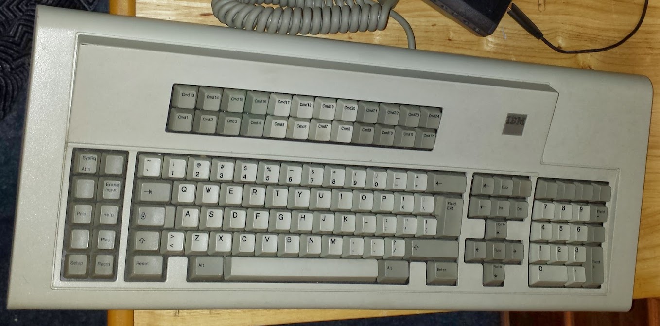
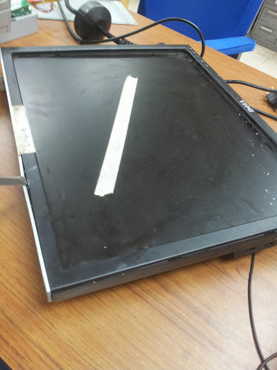
This project was originally started as part of the i3 Detroit OpenAccess control system for RFID entry.  I promise I’ll write an entry on that soon, but I’ve got to shake down all the bugs first.  These displays that I got to play with are specifically 1080-s4-13-x-x, which according to the manual means that our displays have four lines of twenty 5mm characters each, 2-RS485 serial ports, 13 buttons, no memory, and no clock.  Because these are the only two displays I have, theirs are the only features I implemented.

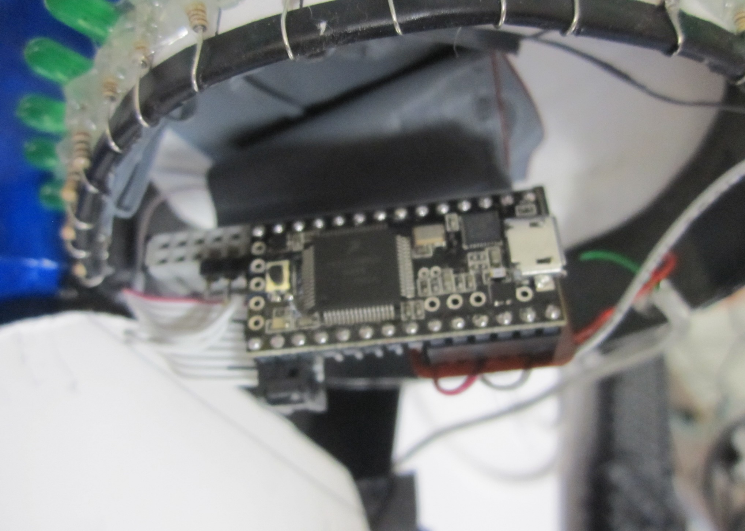
My setup was originally on the Open Access Control 3.0 shield for the arduino mega 2560, this shield has a SN65HVD05 on it’s hardware serial port 3 and has the Rx/Tx pin connected to pin 16.  That’s the thing about adapting an RS232 port to RS485, RS232 is full duplex, meaning it can transmit and receive simultaneously, RS485 is half duplex using one pair of wires as a differential twisted pair for both transmit and receive.   The twisted pair differential signaling is better for noise immunity, but because of that it takes twice as many wires to run full duplex.  The full duplex equivalent of RS485 is RS422, but that’s a less popular standard for a number of reasons.  When adapting RS485 to RS232 the adapter chip has a pin to enable receiving RS485 signals to RS232, and another pin to enable driving the RS485 signals from RS232.  These pins are usually opposite polarity so that one digital IO can control switching from Tx mode to Rx mode.  This particular use of the display only connects to serial port 1.

The following information is just on the features I implemented, some features were not present on the devices I handled, some features I didn’t find useful, and some features I couldn’t figure out, that’s why they weren’t included.

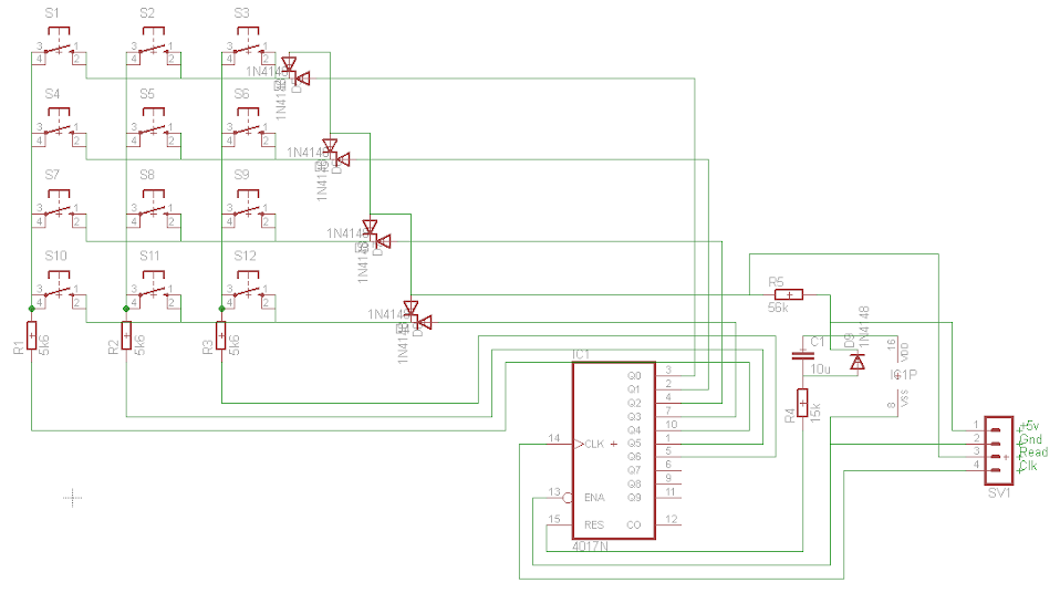
There are two modes I used these displays in: single unit mode, and multi-drop mode.  Single unit mode is exactly as you might expect it, one display connected to one serial port taking commands directly.  The multi-drop mode adds a packet format to the device as described in the manual I have linked to above and the code I link to down below.  In multi-drop mode any number between 1 and 255 can be used as a display address except 4, 4 is the end byte in the message protocol.  These codes may seem arbitrary, but they somewhat faithfully implement the ASCII table’s control characters (start of text, end of transmission, etc…).  The commands for single unit mode and multi-drop mode are the exact same, except the multi-drop ones are wrapped up in a packet with an address in it.

There are four modes for taking input from these displays, we’ll go over them one at a time.

Buffered/half duplex mode allows the characters to be written to the screen at the current cursor position without host intervention and also placed in a buffer, the UP arrow key backspaces, the DOWN arrow key places the down character in the buffer.  The buffer is dumped when the ENTER key is pressed.  I don’t like this mode because it alters the display from a known state without telling the host.

Buffered/full duplex does the same thing as buffered/half duplex, except it doesn’t alter the display.  I don’t like this mode either because you can’t tell if the UP key is pressed, and in order to know when any key is pressed you have to hit ENTER (this also applies to the buffered/half duplex).

Instant/half duplex allows the characters to be transmitted when they are typed, but also puts them on the display.

Instant/full duplex is my preferred mode, it outputs keys to the serial port when they are typed and also doesn’t display them (like an old school dumb serial terminal).

These displays have all sorts of features, I really like them.  One interesting feature is the ability to set any of the functions to any if the available ports (or an internal 800 character buffer).  What I mean by this is the available ports (in my case serial ports 1 or 2, the buffer, or a null port) can be mapped to where the display either takes a specific kind of input, or sends a specific kind of output.  Those specifics are as follows:

Main input port: takes ASCII, control codes, and escape codes.

Data output port: when the display needs to send data to the host.

Key control port: used to send keys to the host.

Repeater port: parrots out the contents of Main input port, for use with long cable runs

I personally didn’t use the Repeater port, and I had everything else set to serial port 1, but there’s something interesting about the Key control port.

Since the Key control port can be set to an 800 character buffer, it can be used to buffer a lot of key presses, but more importantly the buffer can be polled in multi-drop mode to figure out who sent those key presses since you can’t set what value the number keys return.  In instant/full duplex mode with the key control port set to the internal buffer the key presses are stored in a buffer that can be polled by the host (polling each multi-drop device separately so you know where the key presses came from).

The control codes are very striaght-forward, I implemented the following:

0x0C => clears display, sets cursor to home position

0x10 => the text following will be blinking

0x12 => the text following will not be blinking

0x14 => sets the cursor position, although my implementation only allows you to set the line

0x15 => turns cursor on

0x16 =>turns cursor off

By following the examples I have built into the library it could be expanded to allow all the control codes to be used, but I didn’t find the rest useful.

The escape codes are actuated by sending 0x1B followed by a single ASCII character.  I assume the escape codes are different from the control codes because the control codes are implementing the unprintable command part of the ASCII table while the escape codes are able to be entered simply by typing the ASCII character for ESC and another ASCII character at the terminal (something an operator could do).  The escape codes I implemented are as follows:

0 => resets the display

1 => disables the keypad

2 => enables the keypad

5 => bargraph on a given line (and clears out the rest of the line)

B => read buffer

C => clear buffer

In order to use my code properly the displays need to either be in Single Unit or Multi-Drop mode, the keypad needs to be set to Instant/Full Duplex, the Main Input Port and Data Output port need to be set to a serial port (I used port 1) and the Key Control Port needs to be set to the internal 800 character buffer (4).

The functions I have implemented are pretty easy to understand after my explanation here and a quick glance at my example code and the library itself.  The information provided here is for the use of anyone who needs it, if you have any questions feel free to comment.  The thing is, these displays are really expensive, I only got to play with one because it was donated to this project, so most people who use these displays are doing so with “Industry Standard” everything, so they don’t need to know how to talk to them with anything a bit more reasonably priced.  If you should happen across one of these things though, jump on it.  They are easy to talk to (now) and really slick looking.

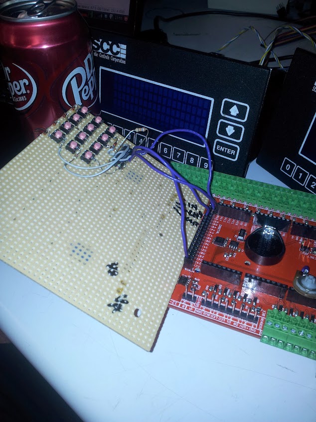
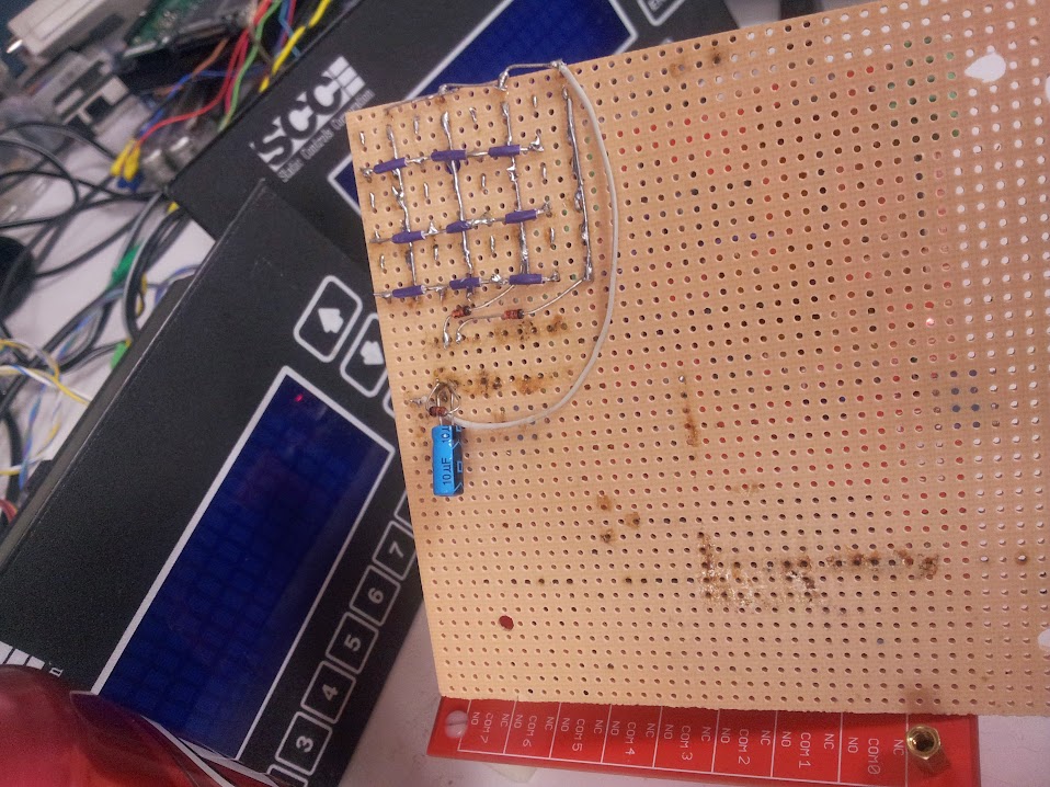
You can find my code here, the READMEs are at least a bit descriptive, some of the test code is old and doesn’t use the current revision of my libraries (or use them at all).  I intend to put up the code for reading buttons very soon (next couple hours) as I only realized the thing about the buffer while writing this.

ADDENDUM: I spent a while with this article written as you see above and attempting to get the button reading working from the buffer.  I couldn’t do it.  I know how it should work (or how I think it should work as the manual I have is different from the firmware on the displays in front of me).  I know that once I post this I will get around to trying again and it will work, but for now it’s being posted with the button reading code non-functional (in multi-drop mode, I got instant/full duplex working with the key control port set to the main serial port, but it’s mostly useful if you only have one display so you know which display sent the button).  And, of course after I submit this is when I will get around to cleaning up the library.  For now common sense would dictate that the higher the number the example sketch, the most updated it is (although I can be counted on to violate common sense at every turn, so take that with a grain of salt).

RFID card ID formatting

July 10, 2013

I keep intending to blog more, and I keep getting side-tracked.  There will be more regular updates after the Open Access Control 3.0 system is hacked together had installed at i3 Detroit, you can follow along with the updates as they are made here.  This update is a small part of that project.

RFID card reading systems have three main formats they return/accept IDs in: 1 26-bit numbers, 2 16-bit numbers, or 7 4-bit numbers.  The first method  is the most obvious, you take a 26 bit binary number and represent it as a decimal value.  This is usually the number displayed on the side of the badge or key fob.  The second method for identification pads the 26-bit number out to 32 bits with leading zeroes, splits it into two numbers, and represents each of them in decimal form (usually with a colon in between them).  The maximum value for this system is 1023:65535, that is a 26 bit number, all of whose bits are 1.  This method for identification has been seen on some older cards and in off-the-shelf RFID door systems.  The last method of representation is to convert the 26- bit number into a 28-bit number by padding it out with leading zeroes and splitting it up into 4-bit hexadecimal digits.  This method is frequently used as a compact visual representation by embedded processors (I use this method, ok).

Example: the above tag reads: 0005280984, that’s the decimal representation.  from that we can easily get the binary representation as: 00010100001001010011011000 (note the leading zeroes that make it 26 bits).  padding this with 6 zeroes we get 0000000001010000:1001010011011000, or 80:38104 in the second notation.  The third notation gives us 05094D8 (note the leading zero).  All this being said, it’s extremely important that you note there are no trailing zeroes in your binary numbers (as in you have more than 26 bits), otherwise your value will be shifted and unrecognizable in decimal or hexadecimal notation.  The code used by the Parallax serial RFID reader outputs in hexadecimal digits (as characters), the code from the wiegand26 library I use outputs a trailing zero at the end of a binary sequence (but it’s stored in a long, no characters so can be rendered as anything), and as such must be shifted back off the number.

4017 based keypad matrix scanner

June 27, 2013

So, here’s  a simple concept I modified to be a lower pin count and fewer processor cycles less.  The original example I found here used a 74hc595, which is an 8-bit shift register) to scan one bit through the register and through some clever trickery with pull ups and pull downs read out serially what row and column that button is in.  My modification did away with the shift register (which you have to prime with one bit every time you scan) and replace it with a decade counter.  The decade counter does just what we’re using the shift register to do, scans one bit out many outputs.  The decade counter can start in an unknown position, but the start up reset circuit (a diode, capacitor, and resistor to temporarily pull the line high until the cap is charged, then pull it low always after that) sets it back to a known state.

I haven’t seen anyone else try this particular setup before, partially because if through some cosmic radiation (or something more likely)  and a bit gets flipped then you’ll be off-by-one for the rest of your days.  This can be gotten around by triggering the reset line before every read, but I’ll try my hardest to keep the pin count down.  The next problem is that the decade counter resets after ten cycles, not eight.  This should be able to be remedied by tying the reset line to the 9th output, but I haven’t had much luck making that work.  The solution  I came up with is to manually clock the device twice after every shiftIn().  My code here makes it easy to implement the keypad polling in whatever code you’d want.  This could be expanded to a 4×4 matrix with minimal modification (it was originally designed for such, but I’m not using one).

The circuit is fantastically simple to wire and to code for.  I didn’t have any circuit board I was willing to sacrifice to this temporary setup so this is some old wire wrap board (no copper).

This was to be used in the OpenAccess system, but it was abandoned like lots of other parts.

Teensy 3.0 based dumb POV globe

June 27, 2013

So, here’s a completely custom design I had, a POV globe done in 9 hours.  The motivation was easy, I am the president of the Michigan Technological University IEEE Student Lab, and we needed to have lots of blinky things to show off to prospective freshmen touring the university the next day.  We had some old stuff, but I had heard that there was a group on campus that couldn’t manage (over a number of years) to build a working POV globe.  I immediately stated that it should be a trivial task and that I could do it easily.  This statement was, of course, met with a suggestion that I should build one… so I did.  This is it:

I have to say that the big seam on the right was closed much better the first time I used it, and the paint jub on the base was done by a friend who wanted to help with the project.

The main parts of this are as follows: a computer power supply, a PC fan, a strip of metal bent into a ring, some foam board for the sides of the ring and the base, a 555 timer based PWM circuit, a Teensy 3.0, a battery, and some LEDs.  First I’ll go over my design philosophy for the base.  The base is literally made of a computer power supply and a PC fan screwed down to it as seen here:

The blades were broken off the fan so there would be no massive air currents or problems caused by having no air to suck up from the bottom.  The metal ring was simply hot-glued on to the ring and balanced so that there was minimal wobble.  The PWM circuit seen closer here:

As you can see, it’s a very simple circuit, I built it right on to a DIP-8 555 timer chip and have had no problem using it this way.  The reason I chase to do a PWM circuit rather than just use a POT as a voltage divider to vary the speed of the fan is that the fan is designed to run at 12v and is most stable (has the most torque) at that voltage.

Now, let’s look at the Teensy circuit:

So there are two things I have to say about this: I know it’s overkill, and the schematic is slightly wrong.  It should have the LED that’s going to pin P13 should go to P16.  I couldn’t figure out why that pin kept outputting data/clocks/noise on that pin, so I just re-mapped the output pins in an array in the code.  It was pointed out to me that if I had latches on the outputs that I could be assured the columns always turned on at the exact same time, but that’s for another later version which I’ll talk about later.

The battery is a cellboost single lithium ion cell + charger + step up converter to output 5v.

I thought it was the easiest solution considering I couldn’t use a slip ring connector to deliver power since the only axle was the PC fan and I wasn’t going to hack that apart any further than I had to for reliability’s sake.

At this point I feel I should address the lack of any timing mechanism.  I didn’t add a timing mechanism for three reasons, one: I didn’t have a slip ring connector to pipe in the tachometer from the fan, and two: I didn’t have a hal-effect sensor handy (the easiest way to get timing), and three: I didn’t have time.  The timing is done simply by setting the delay in the code to a sane value and fiddling with the POT until it processes very little.

Now that I have a spinning blinking thing, let’s pick something to display.  The earth is the most obvious thing that comes to mind, so I did it.  I got a picture of the globe as a Mercator Projection because of the way I placed the LEDs it meant simply dividing the picture into squares and representing the land/water data as binary.  I did that using this picture:

Yes, I did it manually, but hold on, that’s not the worst thing.  once it was represented in binary in code I just had to iterate through the columns and rows and write out the value in the array.  That’s not so simple when you’ve got the syntax for boolean evaluating operators wrong in arduino.  The absolute first revision of the code used one loop, the main loop, and a whole bunch of digital writes.  I feel kinda dumb, but I was also up for about 36 hours at that point.  The final code is here, and the github repo also has some other stuff in it related to this project, like a presentation I prepared to explain what I did.

There’s a glitch in Australia that was fixed in a later revision

I have an updated design that uses a parallel EEPROM and a bunch of discreet logic.  I will have a post about it soon if I can find the paper I wrote it down on.

Rre-purposing an HP laserjet control panel

June 27, 2013

One of the things I salvaged that I didn’t think would be that easy to get working was this HP control panel.  It turns out someone else has already done the legwork to get it working for the most part.  The original source I have for my specific control panel is here.  That site has a really good description of these HP modules, but I can certainly say they are not all the same.  It seems to me that the VFD controller (m66004) is SPI, there is also a shift out register (74hc595), and a shift in register (74hc165).  All of these devices being SPI you can control them all with very few wires.  The module I have has a VFD and 8 buttons, I have an m66004 and 74hc165 on my board.  There is also another version that uses a 74hc595 to drive LEDs as an output.  The arduino library doesn’t need to be modified to remove the LED driver code, but you just don’t have to use the LED output functions.  The board I have also has 9 buttons, one more than the shift register can support.  It appears that the 9th button is connected to the 2nd and 8th button inputs meaning that it cannot be detected independent of the other two and those other two cannot be detected together without incorrectly detecting that the 9th button has been pressed.  The code is 0-indexed, so it’s buttons 1, 7, and 8 that are tied up and button 0 is the first LED.  The demo code has everything in it to demonstrate how to use the functions.  The part I find most interesting is how easy it is made to define custom characters.  Here is my version of the code that does my best to detect the 9 buttons and doesn’t use the LED output commands that don’t apply to my board.  The original arduino library hosted here may have more button functions implemented than mine (there are button isPressed, wasPressed, and wasReleased for people that want to poll constantly or just check periodically).  


Design a site like this with WordPress.com
Get started