Archive for the ‘projects’ Category

Billy mouth billy bass hacking

June 15, 2013

Well, here’s a classic: hacking the old Billy M0uth Billy Bass!  This is an absolute classic, it seems like everyone and their tin dog has done this one.  I picked this thing up at a garage sale, the only intention I ever had was to hack it (who really wants this thing wailing at them?).  Well, let’s get to it.

First things first, the mouth was broken… unacceptable! Let me tell you this thing is a pain to get open, the plaque is fine, but the fish itself… they must have heat sealed it on or something, it looks like a ship in a bottle, like it was assembled inside the skin.  To finally free the mechanics from the skin I put a slit down the back of the tail about 2 or 3 inches long.  Once I got it open it was obvious the plastic had just sheared, lacking patience for 3d printers I decided to just superglue it back together.

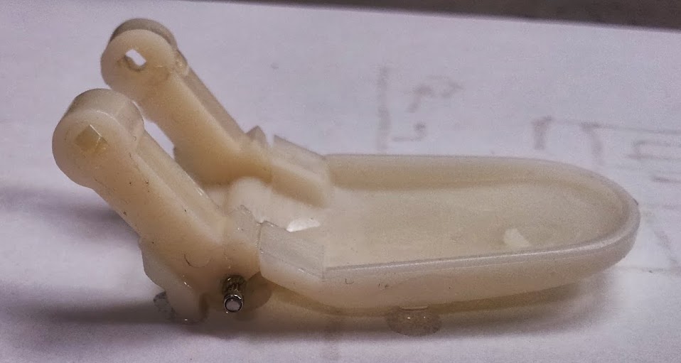
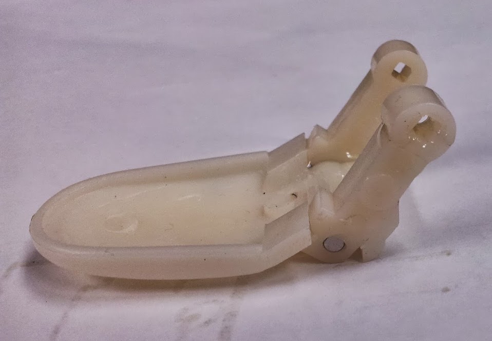
Once I got that glued together I shaved some plastic to get it to fit (I had glued it a bit too tight) and installed it.

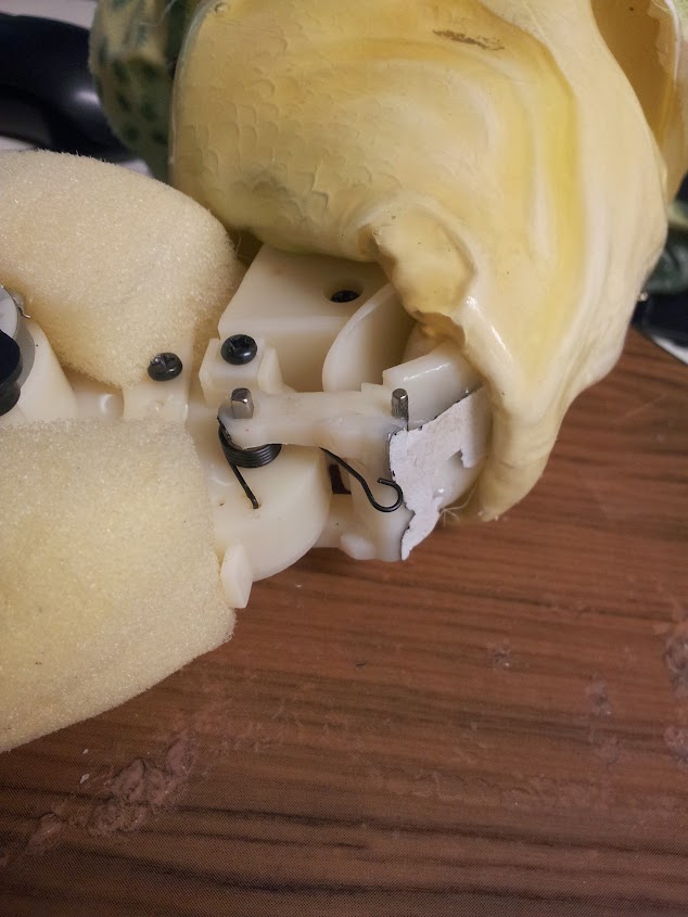
stuck some paper to it with glue…

That pretty much fixed the mouth.  When it breaks again (and it will) I’ll model and print another couple brackets.  Now that that’s done, let’s examine the ASIC.  ASIC stands for Application Specific Integrated Circuit, that means someone designed a specific chip to do this exact job.  In very small runs these are usually FPGAs (Field Programmable Gate Arrays) because of the cost involved in creating an ASIC.  In small runs they are usually like this, what we in the biz call “epoxy blobs”, they just bonded the silicon wafer to the PCB then covered it with epoxy.  In larger runs they are made into standard package ICs.  Epoxy blobs cause such a headache for hackers because the only way you can identify what’s under there is by dissolving the epoxy around the silicon wafer and just looking at.  The more reasonable and down to earth way of identifying what’s in the chip is known as “black boxing” it.  That involves looking at what the chip does, how it reacts to inputs and when it gives certain outputs.  By using a bit of logic you can determine basically what a chip does (while it’s still in the circuit preferably) without needing to know exactly how it does it.

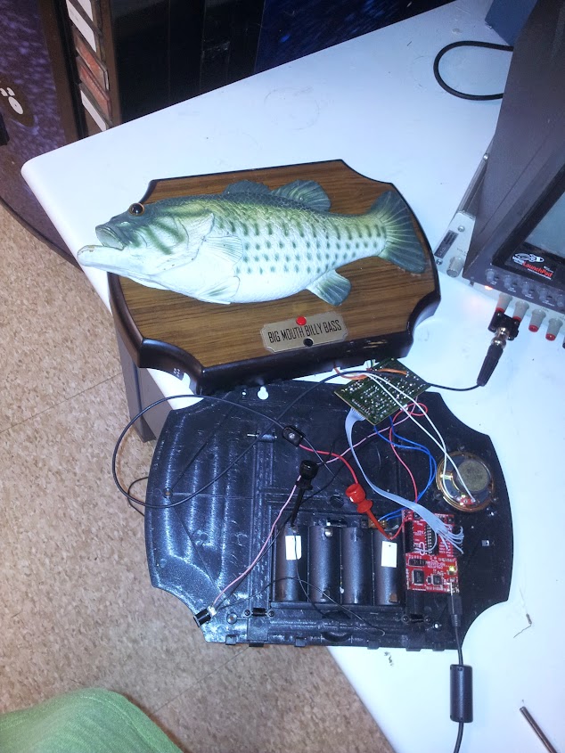
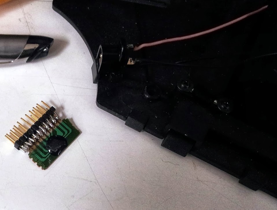
This is the ASIC in question, helpfully it’s on its own PCB mounted perpendicular to the main PCB.  My solution for figuring this one out was to mount the ASIC on 0.1″ headers and stick it on a breadboard, run a ribbon cable and another 0.1″ header and jumper all of them together.  After testing that it behaved the same, I started changing things.  First I verified where ground was (by tracing it out).  Once I had a reference I found (what I assume to be) a relatively stable/regulated 3.3v source.  The next thing was watching what the lines did when the various motors triggered.  That was the single longest time I listened to the built in audio… and I never will again.  The button and CDS cell each seemed to generate analog voltages on two of the pins… kinda.  I say analog voltages, but they’re probably supposed to be digital, but there’s some variance in them, so I use them as analog.  The audio line I left off since I have yet to try to implement this.  Two of the lines I haven’t figured out what they do, but they don’t seem to matter.

Before taking on a project like this I usually say to myself “which will be easier, strategically modifying existing circuitry to suit my needs, or ripping it out and putting in my own?  I usually come to the conclusion that I could certainly build my own controller with a digital input, analog imput, l298d for the motors, but all that work is done for me here.  There is even a nice sorta regulated voltage I can run off of.  In this specific case it was easier for me to ignore how the circuit works (because it’s a mess of resistors, caps, diodes, and bjts) and just try to emulate the ASIC than design a circuit to do this job.  The main reason was that I didn’t want to spend a motor driver IC on this project if I didn’t have to.

The next thing is the brain.  The microcontroller is a key decision, the part that pushed my decision on this one was the voltage, the circuit seemed to run on about 3.5v so that meant I could use an arduino, but only if it was running at 8Mhz (which I didn’t have set up) or I could use an msp430 from one of the launchpads I had kicking around.  I’m not familiar with programming for the msp430, but luckily there is a project to program the launchpads with wiring code (what the arduino uses): Energia.  Slapping the msp430 on it I quickly built this small sketch to showcase all the inputs and outputs.  My eventual plan with this is to get a serial link working so it’s just another peripheral you can interface to with whatever program you want (maybe an ROS module? but that’s an idea for a future project bleeding in).  All images can be found here.

Reverse engineering a rackmount display

June 13, 2013

Well, let’s get on to some real, original hacking (be prepared for some seriously crappy code).  Now, as I’m sure will be a popular theme for a while: I have no idea when I got this thing, nor did I save the motherboard to see where everything was originally hooked up.  Luckily this thing only has 4 chips, all of which fairly straightforward and easy to understand.  Before we get to that, let’s look at the button matrix.

crappy notes (1)

Now, the numbers and letters for the buttons are not defined by the labels on the front, but the markings on the board.

This unpopulated header has the entire button matrix pinned out to it, very useful for testing.  Now that we have the matrix worked out as seen in my really crappy notes, we’ll see where it’s hooked up to.  One side of the matrix goes to an mc1413 (also known as the uln2003a), a very common part, a darlington transistor array.  This chip can be thought of as simply a pass-through as far as the logic is concerned.  Technically it allows more current to be sourced from the logic chips to drive things like LEDs (we’ll get to that later).  The 1413 is connected to a 4017 decade counter, it steps through each of the outputs one at a time.  The other side of the matrix is hooked up to an mc14076, the 4076 is a 4bit register, it allows you to latch in the data, then read it later.  So, so far to just read the buttons (and dip switches) we (re)set the 4017, latch the data, read it, increment the 4017, latch, read, increment…. and it eventually rolls over.  Now how about the outputs?

The display is hooked up as you might expect, the 7-segments are all hooked up in parallel and the common cathodes are hooked up to the 4017.  The 14511 is a BCD to 7-segment driver, that means it can be fed binary data over a 4-bit bus and it directly drives the displays.  The 4bit bus is the same one that you use to read the buttons, even though it has enough pins on ribbon cable to do it with only one-directional pins.  I can assume that the original circuitry it hooked up to either used a 4bit bus, or could only make the 8bit port all input or all output, so there was no reason to use separate pins.  There are only eight displays and ten positions on the 4017, so the four LEDs on the bottom are hooked up to the 7-segment driver so that segments 9 and 10 are LEDs 0 and 1, and 2 and 3.  They are hooked up to the segments so that a zero turns both segments on, a one turns one on, and a two turns the other one on.  Feeding anything but binary 0-9 results in a a blank display (or both LEDs off).  The method for writing to the displays is simply to (re)set the 4017, set the data bus, increment, set, increment, set…

crappy notes (2)

There are a couple of other lines I haven’t n mentioned, first is the one I dubbed “output_line” which switches the register off to allow us to use data lines to output to the 7-segment driver without having the key matrix data corrupt it.  The next is one I have dubbed “colons” because I thought that drove the decimal points on all the displays making colons (since they are  flipped upside down for every other one).  I haven’t gotten that to work yet, maybe I’ll take a closer look at it later.  The whole data read and write sequence I have now goes like this: reset 4017 (only at the beginning, or every time it should be back at the beginning to reset any corruption), set data bus as inputs, set output line high, toggle keypad latch, read in data bus, set data bus as outputs, set data bus all low, set output line low, write data bus with a digit, increment 4017, repeat…

The really clever thing about these 7-segments I only learned after I was tracing this board out, they’re meant to work upside down.  What I mean by that is that the pins mirrored when they are flipped upside down control the segments that are also mirrored,  This means that you can still run the traces on the board almost straight and have them all hooked up in parallel even with every other one upside down.  I always hated the confusing pinout on these thing, but after I learned this I just think they’re absolutely brilliant.  I originally tried to write the button reading pattern from my understanding of the circuit, but eventually I just tried it and re-mapped it manually.  All the chips also happen to work at 5v, so just wire it up and off you go.  My code is on github here, and the rest of my pictures are here.


Pocket TV upgrade

June 13, 2013

the victim

So, adding to my growing list of projects where I add features to things that should have had them from the start, I bring you: composite input on a pocket TV.  This particular TV (Casio TV-890) was made useless by the Digital broadcast television switchover, it has no jack to put in an auxiliary signal, and thus can’t be used at all.  So, since we all know the world runs on some sort of composite video signal (or can be made to) let’s crack this thing open and find us some signal paths.  Maybe we’ll check the pads coming off of the RF can first, maybe look up part numbers for a video chip, maybe…..oh, well that was anticlimactic

unpopulated jack

So, a similar model has a three conductor 3.5mm jack with spdt switch built in.  Presumably this is for video/audio and, yup, it is.  The next question is where am I going to find one of those jacks? how do you even source a part like this? Well, I just so happen to have one, no idea where it’s from but I have one close enough.

salvage part

Now, some of you may notice mine is a dpdt switch, yup, and I only have to re-locate one capacitor to make it fit.

moved a cap (always with the cat5…)

But, there’s another thing.  On the underside of the board there are two zero ohm resistors jumping the contacts that would normally be connected on the jack that isn’t present (for reliable operation they should be removed, otherwise you’re back feeding the RF stuff, or getting signal mixing).  What I mean by that is: these types of jacks sometimes have, say, 5 pins when you might think they only need 3.  Obviously you need audio, video, and ground (or left, right, and ground in the case of an audio application) but what are the other 2 pins for? They’re pass through audio lines.  Think back to a set of speakers that stops playing when you plug headphones in, that’s what’s going on.  When you don’t have headphones in, the audio gets routed through the pass through pins into the speakers, but the physical act of plugging in headphones breaks the connection and the audio is routed to your headphones.  This is used in the opposite way, in the sense that you are routing a signal into the TV, rather than out.  The use of a separate switch may be to cut power to the RF components so power isn’t wasted while they are not in use.

two tiny zero ohm resistors that are clearly jumpering pads meant for a jack

Well, what can I say? It’s not much of a hack. It works, or, it did.  I think I was slimming it down for use as a portable screen for something or other and I broke it, so there isn’t a picture of it working, but I swear it did.  Oh well, at least I got to tell people how to upgrade theirs.

entire album

Simple headphone splitter

June 12, 2013

my simple mod

Anyone who is familiar with computers tends to know that on the back of most motherboards is a little tower of headphone jacks.  This connector (usually 3, sometimes 5 or 6) is a nice way of bundling all the needed analog audio outputs of a computer together, but if you’re salvaging parts from an old or dead motherboard why would you take it? it has a strange footprint, it’s seldom you need 3 outputs from a project, and even less likely that you’d use it to repair another motherboard.  Here’s a simple use for it: a headphone splitter.  I personally use mine to go from my hardware master volume control to my speakers, wireless headphones, and 5 1/4″ bay speakers.  Another mod I did was to take one of these and wire it up so one was pass through, one was mono left and one was mono right.  That particular mod was nice for a dual monitor computer with speakers built into each monitor.  These connectors usually have leaf switches built into them so the audio path is disconnected and redirected out the jack you just plugged into.  The possibilities are not endless, but they’re certainly more than I have stated here.  I can post a diagram of the pinout I derived, but you’d be better off with a continuity meter and a 3.5mm plug.

LED backlighting a 22″ lcd monitor

June 12, 2013

This one’s kinda messy, but I was visiting my parents so I only brought my soldering iron and basic tools with me.  I had a friend mention that their lcd monitor was broken, of course the first thing out of my mouth was “I can fix it no problem”.  It was a little more complicated than I thought.  Let’s review the most common failure mode of electronics this decade: bad caps.  What I mean by that is capacitors that have failed, exploded, had their ESR go up, heated up due to that and then exploded, or bulged, or just plain leaked.  The reasons are numerous: there could be an unexpected cooling failure causing the caps to heat beyond their tolerances; there could be too high an ESR as I mentioned; they could even just be, gasp, old! But by far the most common reason for failure is espionage.  It’s a little more mundane than it sounds, there are news articles, wiki entries, and even a website and forum dedicated to it.  I’m just hereto say it has been a godsend for those of us that can open consumer electronics and solder reasonably well.  When you have people throwing out devices worth several hundred dollars each because of a few cents in parts that are fantastically easy to identify and fix… well, let’s just say I know some people who could major in monitor repair and minor in general debugging.

the whole setup, mountain dew and all

This problem monitor happened to be a Sceptre 22″ lcd monitor.  Now, due to the rapidity that people are throwing out monitors I tend to have a large backlog from which I can pull parts (usually entire power or logic boards, sometimes button panels, etc…) but I don’t have any spare dead monitors this big.  Once open (although I should have done this first) it was obvious that the LCD worked, the logic board worked, and the main part of the power supply worked.  I could tell because the only thing that didn’t work was the back-light   This doesn’t preclude it from being bad caps, but it lowers the likelihood   In back-lights I tend to see one of four things go wrong.  First there is the simple bad caps on the inverter input, this wasn’t the case here.  Next there’s the blown PWM chip or blown FET driver, usually SOT-8 or DIP-8, can be blown by heat, time, or voltage fluctuations (sometimes traced to caps). Another potential failure mode I know is shorted transformers; I haven’t ever gotten a monitor I cared enough to diagnose this far, but the PWM chips create a square wave that gets stepped up in the transformers to drive the high voltage tubes.  The problem this time was bad back-light tubes.  These tubes were seriously blown, though I have come across ones that glow red briefly and then the over-current protection kills the back-light inverter.  Well, I don’t have any spare tubes this size, what about LED strip lighting? that should work, right?

assembled with strips installed

I ordered a 12v LED strip off of amazon and it is pretty nice stuff.  The stuff I bought had a rubberized coating on it meant to be used outside, which didn’t really help, but oh well.  The rest of the mod went as expected, I pulled the tubes, carefully disassembled the panel and fitted the new lights, ran power wires through a switch because I didn’t feel like working out the back-light auto-on feature and powered it off of the 12v tap on the power board.  That simple, I could have done with some better diffuser  but I didn’t have much time to work on this.

monitor off, back-light on, diffusion problem

working. Next patient!

entire disassembly album

Modded slug

June 12, 2013

This is in no way an original project, but I’m publishing it because I think some of the things I did were pretty neat.  A long long time ago Linksys released the nslu2, a network atatched storage device.  That’s cool, let’s open it up to see what it has inside.  TTL level serial port, cool, I put a header on it, and broke it out to the ftdi friend standard with a pigtail though a hole in the case.  Overclocking? yes please! just remove resistor R83, it’s that simple to double the clock speed.  now you’re cooking with gas at… 266Mhz. Ok, this is a bit of an old device.  What else do we have…. more USB ports? ok, I can break those out, but first what’s with this one port that doesn’t allow flash drives? it has no power line soldered to it… what? Ok, there’s a set of pads for a fuse like the other port has, but it’s not connected.  Maybe it’s to make sure their cheap power brick won’t crap out on them? No matter, solder a jumper and it’s done, add another 3 ports and they’re all broken out.  The thing is, I didn’t have 3 nice USB ports at the time, but I did have an old USB PCI bracket that’s normally used to break out motherboard USB ports.  No problem, just grab some pin header and a scrap of PCB (these pin headers tend to fall apart if not soldered to something sturdy.  Now I have a total of five powered USB ports.  Now, about that power adapter… This thing runs on 5v, and after tracing the power rails I find that it’s unregulated all the way out the USB ports, so I dig out a monster 5a 5v supply, graft on the right barrel jack and we’re in business.

new ports soldered in, pretty cleanly

Ok, now that we’re done with the hardware (all that I did anyway) let’s move on to the software.  I’ll admit that I had modded this thing, put it on a shelf and forgot about it for a while, the only thing I remember was insisting that I had to have the most capable linux install on it (a debian derivative) and it had to be a fully featured linux box (a configuration nightmare compared to what I finally used it for).  So I have a modded slug that I want to re-mod to have Unslung on it, a derivative of the stock firmware that allows those extra usb ports.  All the tutorials say to “use this utility and it’s easy”, bah, I have a serial terminal, no need to mess around with blind boots, and all this crap.  With my experience modding FONs and other embedded linux devices I’m actually more comfortable with redboot, a tftp server and raw commands.  Following the tutorial listed here I got it installed and booting in no time.  I can’t use it as a general purpose webcam server or network connected speaker system, or whatnot but it’ll make a good NAS.

big boy

There’s another interesting feature of the nslu2 has, a strange one, a USB device port.  Now, I can’t really say what I’d use it for, but it’s there and I haven’t done it yet (I may never).  There is a mod to auto power on the slug using a capacitor (The same hack can be done with a desktop, I think) but I haven’t done that mod, mostly because I have real servers… also does this thing not respond to WOL packets?  Now, looking at what people have done, using it as a network attatched power switch and stuff, they all seem to use usb connected devices to trip FETs or relays… what about the activity LEDs? can you not manually control them like on the WRT54g or the FON?  Some pretty fantastic things have been done with these devices, as a EE I tend towards the really cool hardware, like using the I2C bus to talk to low level devices directly, adding more RAM and flash, and the fact that there is a second RX and CTS only serial port in there somewhere.  Check out the wiki, it has so much covered on this neat little gadget.

done

References:

pretty comprehensive wiki

fantastic pictures

DIY hard drive toaster

June 12, 2013

So, here’s an old one, anyone else do enough with sata drives that warrants having a way to easily and painlessly drop one in a computer?  I did,but I really couldn’t justify one of those hard drive caddys, they cost a lot more than the regular enclosures I had lying around (buy a hdd on sale, pop it open, drop it in on a sata bus for faster transfers).  The idea is pretty simple, it just has to hold the hard drive firmly and be able to be removed at a moment’s notice.  I really liked these Western Digital MyBook drives, they fit on a shelf, are easy to open and they stand up, which is important for this mod.

the finished product

Construction: cut it in half.  Well, ok, it’s a little more involved than that.  Pick a spot (probably above the light pipes is a good idea), measure it out so you have a level line all the way around, and cut the outer plastic.  Now you have the inside metal caddy to deal with, cut it a little below the level of the outer plastic to allow for a nice top to fit level.  The top came from the discarded top of the MyBook, but it curves, and mine doesn’t.  You  could curve yours right along with it, but I cut mine off right before the curve and used the bit salvaged from the back to complete the top.  Now, just cut a hole in the top the right size, slather it in hot glue and you’re done.  The reason I say hot glue is that all the methods this thing had for staying together are now compromised, like cutting the top off of acar: you need to reinforce it, or it’ll fall apart.  There you go, don’t forget the light pipe before hot gluing the hell out of it!

as you can see, I used the bit of caddy to reinforce the other side

The rest of the pictures

Upgrading the tl866cs, or: misadventures with PICs

June 12, 2013

So, as the story usually goes: I bought the crippled cheaper version and dropped way too much time upgrading it. This time it’s the tl866cs EEPROM programmer. but this thing is much more than that, it does reading and writing of EEPROMs, sure, but it also does avr, pic, 8051, PLDs, all sorts of stuff. The part that sold it for me was that… well, what do you think this programmer is? it’s a micro with IO expanders (or at least buffers), and digitally configurable voltage regulators. so, crap-tons of IO, definable power and ground pins… this thing can test piles of logic chips! all you have to do is apply input signals, take output signals, check against a known good and report faults. So it also tests 7400, 4000, and even ram chips. So this thing is an absolute godsend, it has tons of chips in the database, hex editor built in, configurable pretty much anything.

Now, on to the differences in the versions. I bought the tl866cs variant which has the 40pin zif socket, but no ICSP connector. Don’t get me wrong, it has the cutout, has all needed passives, just needs the header. The full version is the tl866a, what I wanted to upgrade to. Now, as far as I can tell this is an original Chinese design: I don’t know of another programmer in a similar form factor, they have their own GUI (unlike the Saleae I modded the other day). They are understandably hesitant to release any schematics, firmware, or even what chip is driving the entire thing.

Let’s start with the chip. They have scraped the part number off of the package (rotary tool of some kind) and apparently thought this was enough. I won’t even go into the brute force method which starts with the USB Vid is licensed to microchip if I’m not mistaken and they have this wonderful thing these days where you can sort by package to get all possible PICs in that package, then trace power, ground, ICSP, and crystal and you have the family, if not the exact chip (oops, I guess I got into it). The really hard way involves acid and building a complete picture of all it’s specs based on the silicon die, but we’ll save that for military ASICs (You can’t hide from us!). The easy way is to ask around other people who bought it (they are probably electrical engineers/hobbyists, who else buys no-name Chinese stuff like this) and find someone who can read the slightly less worn away chip they got in theirs. Now we have the one unknown part we can proceed to reverse engineer a schematic pretty easily. I know it’s time consuming, but luckily we can outsource that job to people on the internet with more free time than us.

bottom featuring shaved IC and it’s ICSP header… facepalm

Just a side note on the construction: this board is designed fairly well, I only have a few gripes. It seems fairly obvious that these PCBs are machine assembled and the final product is hand assembled. They use standard 0.1″ pin headers to connect the boards and solder wires to hold them in place. My main gripe is not the wires, they’re redundant grounds, my gripe is those darn LEDs, they are on long leads that go all the way through the boards and solder in the bottom. You’re already putting in all those pin headers, you can’t put in 4 more pins!?

modular pin headers… thank god

Ok, now that we have the hardware, let’s move on to the software. This is where I got hung up, bored, and let someone else do it. We’ll start with my attempt. First thoughts: different USB Pid for each model (so very wrong). we’ll skip my pawing at the minipro files looking for plaintext and move right on to the fact that someone actually discovered that there is a bootloader that takes firmware updates, the firmwares are encrypted, and the bootloader checks them on boot to see if they match. They also decrypted them, reverse engineered the bootloader, created an application to generate bootloader and whole firmware unencrypted hex files with user settable IDs…. duuuuuude, so much work, such nice documentation.

my original serial and dev codes

Now, looking into the future, there is also talk about creating custom chip libraries and chip testing/programming algorithms…. I envision a utopia future where there is a crowdsourced effort adding chips to the library, maybe even designing better hardware (using digital pots to get finer power control than 8 distinct voltages). but I digress…

boost converters on the left

OK, now I have a firmware image to write to the PIC, all I need to do is whip out the pickit3. Oh, I don’t have one. pickit2? Nope, hmm, I have something for PICs around here… AH! here, a microchip mplab ICD 2. Ok, no problem install mplab, and visual studio? I don’t care, whatever, just install it. OK, now how do I set it up? uh, ok, select programmer, blah, blah, error… huh? Well the programmer failed the self test, but nothing’s plugged in to it and it says it passed the test in the settings menu. Uh, we’ll just ignore that. now connect it, import the hex, set the config bits from the hex, aaaaand crap. it can’t recognize the PIC. I don’t know why, the voltages are all fine, it says it’s supported, please work? No, ok, well screw you too mplab. how about some 3rd party pic programming tools. None support this hockey puck of doom. Ok, fine, just use the easy serial programmer. It’s only like five components and I’m in a well stocked lab and…..you want WHAT now?! an 8.2v zener? no I don’t stock those. hmmm, how does this even work… OH GOD, uh, we’ll just forget how they’re doing that voltage regulation… and floating grounds… ok, here’s a more sane one, still needs a 12v zener, that’s ok, I actually have those. Get it all breadboarded up and find out that my 3rd party client supports the PIC18f87j50… with only one of the many compatible programmers he listed. Fine, what else? ok, here, a parallel port programmer, it doesn’t get any more simple. so I need a 74<cough><cough>05, yeah, I’ve got one somewhere, I’m sure it’ll work just fine. Oh, hmmm, it says I need a Vpp of no more than 3.6v, and I think I need logic levels to match. fine, I’ll just lower the voltage on this buffer chip…. crap. it doesn’t go low enough. This is the point where I considered breaking out the textbooks to build level shifters out of BJTs to get the right voltages (I would have already built a pickit2 clone as they can be programmed with the serial thing, if I had the right model PIC for the brain). I just know these chips will work out of spec, what is it Scotty said? “A good engineer is always a wee bit conservative… at least on paper”. Ok, let’s do it. Doesn’t detect programmer… crap. well, it’s breadboarded up, I’ll just… oh… that’s how it checks for this simple programmer, it uses a free input pin to sense the inverse of one of it’s own signals and twiddles it to be sure that, yes, it really is seeing it’s own tail wag. and the pin fell out. Ok, back in, click button, YAY! the programmer is recognized. ok, connect the PIC… one of the pins isn’t used… the one with the bjt… nope, I don’t care anymore, leave it off, keep on trucking. Dump the chip. well, it’s not throwing an error, and it seems to have autodetected the PIC. (yes, hooking up a programmer is exactly all it takes to bypass the ‘scratching off the number’ routine since they LEFT AN ICSP HEADER FOR THE MAIN PROCESSOR OPEN AND PINNED OUT RIGHT). Ok, well, it read something, mostly blank, must be the DRM flag set. Now write the-WARNING CONFIG BITS NOT SET IN THE HEX-. Yeah, they are. No seriously, I open up mplab and import the hex and they’re right there. <sigh> check flag… set flag… check flag… set flag… ok, all are finally set, let’s program. Programming, cool. Errors with verifying, not cool. Well, dump it again, see if it still hasn’t been programmed. No, there’s something different there, quick see if it matches the code I tried to write! huh, slightly different formatting, whatever, where’s the USB cable, plug it in, aaaaaaaand……… SUCCESS!!!!! it is now a TL866A! ok, box it up, now where did I put that AVR ICSP header adapter I made like a month ago…. and it works, no support for the atmega1280 or 2560, but it’ll come, maybe, eventually. this took…. 6 hours, maybe 7? whatever, now I have a decent PIC progammer, never need to do that again.

the setup that finally worked

no, it’s not cracked in half, but it does have 5 or 6 pins repaired with solid core wires.

References:

EEVblog thread with all the wonderful info (starts on page 5 or 6)

programmer I used

software I used

rest of the pictures

Re-using bits from a dead sump pump

June 11, 2013

So, after an evening of hysteria when the sump pump failed and I spent what seemed like forever disassembling my shelves/desk that I had built over top of the sump pump hole in the basement I had some parts left.  Now, I originally had my doubts about what this odd pass-through plug on the sump was, and I should have guessed, there is a float inside that connects or disconnects one line, all the current runs through that switch, then runs the pump.  This means that it is a pass through with 2 wires that come from it that, if connected, will allow the device to turn on.  So, hook it up to a switch rated for wall current, or a pull cord…

there we go, in line power switch. why does no one make these?

UPS Buzzer Removal

June 11, 2013

So, this is an old one.  What happens when you only have an ancient laptop with a dead battery and you still want to go around a convention?  Bring a 120vac battery with you of course! You say you don’t have one? how about a UPS? oh yeah, I went there.  so, the main problem with this is that a UPS doesn’t know you are trying to use it as a battery and it insists rather loudly that it isn’t plugged into the wall and you should rectify that soon.  By that I mean it beeps rather loudly using a piezoelectric buzzer.  The simple explanation is to remove it, the same way I did with my old thermostat that beeped every time you changed the temperature and I got yelled at for messing with it.  That’s exactly what I did, and apparently this isn’t such a novel idea, I recently heard an interview with Jeri Ellsworth saying that she needed to do this to get an extra few hours out of her laptop on a plane.  The concept is simple, here’s the pictures.

really old fuzzy picture

working! (compaq armada 7800, I think, still working today as my 1541 disk drive emulator)


Design a site like this with WordPress.com
Get started